Abstract
Since the advent of Organic Electrochemical Transistors (OECTs) back in the 80s, research focus has shifted from understanding the working mechanism and expanding the materials library to fnding new applications and building larger integrated circuits. Given the strong dependency of these devices’ performance on their geometrical dimensions and considering the increasing need for larger scale and low cost fabrication, research on novel processing methods is paramount. Here, we review the most common processing techniques used for OECT fabrication, starting from classic methods such as spin coating and electropolymerization to more recent and complex ones like orthogonal lithography and 3D printing. We also provide a brief outlook on how these techniques are enabling integrated circuits and large scale circuitry in general.
Introduction
In 1984, White, Kittlesen and Wrighton presented the frst Organic Electrochemical Transistor or OECT.Ever since then, OECTs have developed rapidly, especially because of their advantages for bio-electronic applications. Their hightransconductance enables an efcient transduction of ionic into electronic currents, making the device an ideal mediator between biochemical redox reactions and microelectronics.Furthermore, OECTs are promising for sensing applications,and their bio-compatibility makes them ideal candidates for implantable or even edible electronics.
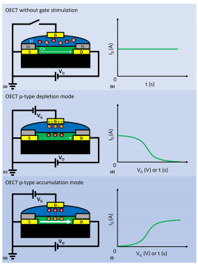
The depiction of an OECT can be seen in Fig. 1(a). These devices consist of drain electrode, source electrode, gate electrode, electrolyte and channel. Commonly, organic materials called Organic Mixed Ionic-Electronic Conductors or OMIECS are used as channel materials. As the name implies, mixed conductors permit both ionic and electronic fuxes in their volume. Generally, for OMIECs applied in OECTs, electronic fuxes occur through the polymer backbone while ionic fuxes take place in the free space between polymeric chains.
To exemplify the OECT doping mechanism, a p-type or hole conducting channel is considered in the following. In the absence of a gate bias ( VG ) and presence of a constant drain voltage ( VD ), both cations and anions tend to stay in the electrolyte, thus resulting in an undisturbed drain current ID [cf. Fig. 1(b)]. Upon application of a positive VG , cations are pushed into the p-type channel [cf. Fig. 1(c)]. As the cation density increases in this region, holes are extracted through the drain electrode, thus reducing ID (de-doping) and confguring the depletion mode of operation [cf. Fig. 1(d)].Conversely, when a negative VG is applied, anions enter the channel [cf. Fig. 1(e)]. With increasing presence of these negative charges, more holes are injected into the OMIEC to achieve charge neutrality. As a consequence, ID increases (doping), confguring the accumulation mode of operation [cf. Fig. 1(f)]. A representation of n-type OECT operation can be seen in the Supplementary Information (cf. Fig. S1).

Figure 1
These challenges sparked research into alternative deposition and structuring methods to process and integrate OECTs. One of the most promising methods was developed by A. Zakhidov.He proposed to use fluorine based solvents and resists that not only are orthogonal to standard resist systems, but are benign to organic semiconductors for structuring, and was able to reach sub-micrometer feature sizes in one of the most heavily used mixed conductors, PEDOT:PSS.
A few more promising results have been reported for n-type small-molecules OMIECs through ethylene glycol (EG) side chains modifcation. This strategy has been used for derivatives of fullerene, perylene diimide (PDI), and naphthalene bis-isatin (NB), to cultivate the following novel molecules, namely 2-(2,3,4-tris(methoxtriglycol) phenyl) fulleropyrrolidine (C60-TEG) for fullerene derivatives, PDI- 3EG, 4Cl-PDI-3EG, and 4Cl-PDI-4EG for PDI derivatives, and gNR and hgNR for NB derivatives. Except for C60-TEG, the use of these molecules in OECTs lead to satisfying drain current modulation with ON-OFF ratio in the range between 103 and 8 × 10⁴.
Electropolymerization
The deposition of electrically conductive conjugated polymers can also be done via electrochemical polymerization. In this method, a monomer is dissolved in a suitable solvent containing a doping anion salt. The monomer is oxidized at an electrically conductive electrode surface by applying an anodic potential resulting in the growing of a polymer flm.
The most famous conducting polymers grown by electropolymerization are polypyrrole (PPy) and poly(3,4-ethylenedioxythiophene): poly(styrenesulfonate) (PEDOT:PSS).The main advantage of the electropolymerization method is that the coating of the polymer takes place only locally at the conductive electrode surface, thus an additional structuring of the deposited flm is not needed. The disadvantage is, however, that this deposition method requires a conductive surface, where the formation of the polymer can start. Therefore, the method is often used for additional coatings of electrodes e.g. for neural interfaces to increase signifcantly the electrode capacity, which enables electrical neural stimulation.
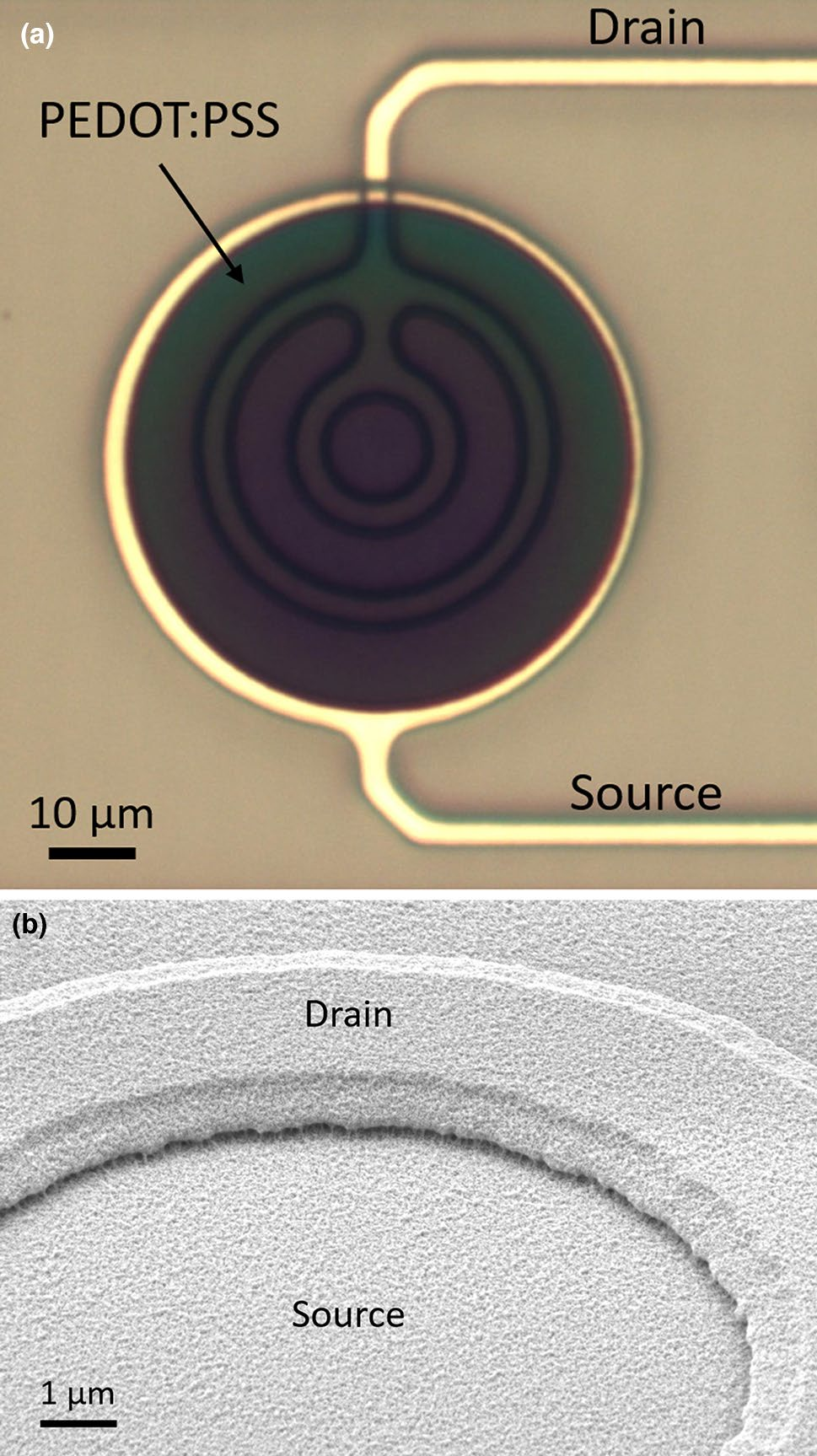
Recently, we established a microfabrication process to create vertical OECTs using electropolymerized PEDOT:PSS thin flms. Therefore, a 300 nm thin polyimide insulation layer is sandwiched between the circular source and ringshaped drain electrode, both made of sputtered gold [cf. Fig. 5(a)]. After defning the area for electropolymerization by coating and structuring another polyimide insulation layer on top, the PEDOT:PSS flm is deposited by applying an anodic potential at the source and drain electrodes, which are short-circuited. Figure 5(b) shows an SEM image of the structure after electropolymerization. The small gap between the source and drain electrodes is bridged by the PEDOT:PSS flm, which is creating the efective OECT channel. With these devices we measured max. transconductance values up to 90 mS, which are limited by the parasitic serial and contact resistances.

Figure 5
Conclusions
Organic Electrochemical Transistors have come a long way ever since their invention.In the past, most progress was made in optimization of materials and individual device performance, alongside a furthering of understanding the working mechanism and modeling of the device.
With growing maturity, translation of this progress into realworld applications has shifted into the focus of research. Integration of OECTs, however, is a balance of several, sometimes competing requirements. OECT behavior depends strongly on its geometric dimensions, in particular the thickness of the transistor channel, which requires a high flm homogeneity and structuring fdelity. Furthermore, organic mixed conductors, as used in OECTs, are fragile and often damaged by conventional lithography. Lastly, OECTs are often labeled as low-cost technology, and in order not to compete with other technologies, have to be prepared without involving cost intensive processes.
上一篇: 微型超级电容器电极材料的最新进展
下一篇: 现代碳化硅功率器件