Abstract
In this work, p-type silicon substrates were etched and coated with graphite paste to form layers of n-type silicon carbide by plasma-induced bonding technique. The structures and morphology of these structures were introduced by x-ray diffraction (XRD), scanning electron microscopy (SEM) and atomic force microscopy (AFM). These tests confirmed the formation of nanostructured SiC layers on the etched Si substrates. Electrical characteristics showed that the formed n-SiC/p-Si anisotype heterojunction has an ideality factor of 0.45 and the built-in potential was measured to be 2.6V. This technique is reasonably efficient, low-cost and reliable to fabricate heterojunctions from nanostructured compound semiconductors on silicon substrates.
1. Introduction
Recently, silicon carbide attracts a lot of interest by research works due to its intensive use in hightemperature, high-power and high-frequency applications. This compound semiconductor is increasingly replacing silicon in micro-electro-mechanical systems (MEMS) and nano-electromechanical systems (NEMS) operating in harsh environments, and too many devices used for automotive, petrochemical and aerospace applications. This material is effectively used in nonoxide ceramic applications.
Silicon carbide is a polymorphic compound that can be found in 200 polytypes and crystallographic configurations. It is a wide-band-gap semiconductor (2.3-3.2 eV). It has high breakdown electric field, high thermal conductivity, relatively high oxidation resistance, high chemical stability, high hardness, high melting point, high electron mobilities and low intrinsic carrier concentrations, which lead to stable electronic properties in harsh environments.
2. Experiment
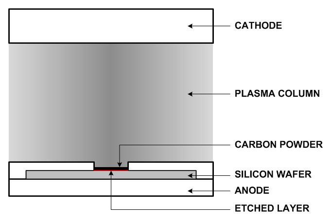
A p-type (100) orientated silicon wafer with resistivity of 15–20 cm , diameter of 5cm and thickness of 650 μm was used as substrate. The wafer was cleaned using 5% HF solution and acetone. Then, it was placed on a flat stainless steel disc with a diameter of 6cm and thickness of 5mm and then mounted by a similar stainless steel disc with a central window of 1cm diameter, as shown in Fig. (1), which was completely covered by the generated plasma column. This assembly represents the cathode of glow discharge system while the anode was a stainless steel assembly of the same dimensions. The deposition chamber was first evacuated to 10-6 mbar to remove any residual gases and contaminations in order to prevent the formation any silicon compounds (especially SiO2) other than silicon carbide. Highly-pure (~99.9%) argon gas was used to generate the discharge plasma.

Fig. (1) The expwerimental arrangement used in this work.
The silicon wafer was etched by plasma at gas pressure of 0.08 mbar, discharge voltage of 1.5 kV and discharge current of 20 mA for 30 minutes to form nanoscale rough surface (~4nm) over the area exposed to the plasma column. Similar work was previously performed by author. The polarity of discharge electrodes was converted and the central window was then filled with a 100-200 μm thick layer of carbon (graphite paste of 25μm grain size) to reach the nano-scale rough surface of the silicon wafer. The sample was processed by plasma generated at gas pressure of 0.15 mbar, discharge voltage of 3.5 kV, discharge current of 45 mA for 5 hours. The sample was cleaned by HF and HCl to remove the graphite particles may reside after processing with plasma. The thickness of SiC layer was measured by ellipsometry method and found to be 90±5nm.
The x-ray diffraction (XRD), scanning electron microscopy (SEM), atomic force microscopy (AFM) tests were performed to introduce the structural characteristics of the fabricated structures. As well, for photoluminescence (PL) measurements, a He-Cd laser beam with a wavelength of 325nm was used for the excitation and the photoluminescent light was dispersed using a double grating spectrometer with focal length of 500 mm and detected by a photomultiplier. With this setup the resolution in photon energy is better than 0.5 meV.
3. Results and Discussion
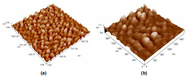
Figure (3a) shows the AFM topography of the plasma-etched silicon surface before covered with carbon powder. The root-mean-square roughness (Rr.m.s) of this surface was reasonably decreased, as shown in Fig. (3b), after the formation of silicon carbide layer, which was induced by plasma.

Fig. (3) Topography of bare etched silicon layer (a) and grown SiC layer (b)
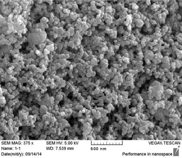
In order to confirm the formation of SiC nanoparticles, the final sample was characterized by SEM, as shown in Fig. (4), and an average particle size of 50nm was determined. Despite the high purity of the formed nanostructure observed from Fig. (4), very few agglomerations can be observed and attributed to the thermal effect of plasma processing, which is reasonably a random distribution of thermal energies over the volume of plasma column. The temperature at the processing area was measured to be 500°C.

Fig. (4) SEM micrograph of the SiC layer grown in this work
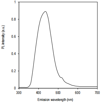
The photoluminescence (PL) spectrum of the fabricated SiC sample is shown in Fig. (5) and obtained at an excitation wavelength of 325nm. Visible PL has been observed from these systems, which opened up the possibility of the integration photonics with silicon-based microelectronics. The PL arising from most of these materials is located in the red or yellow-green spectral region. There were two photoluminescence bands observed at 435 and 535nm corresponding to photon energies of 2.85 and 2.32 eV, respectively (energy band gap of SiC is ~2.4eV). Also, a blueshift of ~15nm was shown and attributed to the fact that the smaller particles of SiC may be a source for such shift as these particles are not easily oxidized at room temperature.

Fig. (5) PL spectrum of the SiC sample grown in this work
4. Conclusion
According to the obtained results, an anisotype heterojunction was fabricated by the growth of ananostructured layer of n-type silicon carbide on a p-type silicon wafer. The growth of this layer wasinduced by argon discharge plasma. The structural characteristics showed that the grown laver is _-Sicwith an average particle size of 50nm. There were two photoluminescence bands observed at 435 and535nm corresponding to photon energies of 2.85 and 2.32 eV, respectively. The electrical characteristicsshowed that the fabricated heterojunction has approximately linear behavior in the forward biascondition, the maximum dark current is about 145wA, the ideality factor is 0.45, the junction is abrupt and the built-in potential is about 2.6V. The technique employed in this work is reasonably efficient, low cost and reliable to fabricate heterojunctions for high-temperature electronic devices.