Abstract
n-TPA-IFA organic material was synthesized and deposited on p-Si by spin coating method to produce n-TPA IFA/p-Si heterojunction diode. We determined that the dielectric constant and energy band gap of TPA-IFA organic material were 3.91 and 3.37 eV by DFT/B3LYP/6-311G(d,p) method using on Gaussian 09 W, respectively and the carrier type of TPA-IFA organic semiconductor material was also n-type at room temperature from temperature-dependent hall effect measurements. Using forward and reverse bias measurements in the dark and under various light intensities, we examined the key electrical characteristics of the n-TPA-IFA/p-Si heterojunction diode, including and n. It was determined that the rectification ratio (RR) was approximately 104 . The reverse current's observed increasing behavior with increasing light indicates that the produced heterojunction diode can be utilized as a photo-diode, detector, or sensor. The photodetector properties of n-TPA IFA/p-Si heterostructure were explored at different light intensities, and the photoresponsivity (R), photosensitivity (PS), specific detectivity , and linear dynamic range (LDR) of the heterojunction found to be changed with reverse voltage and light intensity. It was found that as light intensity increased, the linear dynamic range (LDR), a crucial characteristic for image sensors, increased as well (10.15 dB and 18.84 dB for 20 and 100 mW/cm2 ). Ultimately, the findings confirmed that the TPA-IFA-based heterojunction diode could be obtained for the photodetector application.
1. Introduction
The potential primary advantages of organic material-based electronic and photoelectrical devices, such as their low cost and easy preparation processes, versatility, and ability to cover large areas, have led to a significant increase in research interest in recent decades. Due to their superior photoconductive capabilities and exceptional thermal and chemical stability, organic semiconducting compounds have been used extensively in photoelectric and electronic devices are used in optoelectronic devices. Organic D-π-A conjugated systems, composed of donor (D) and acceptor (A) groups linked by π-bridges, have received significant attention in various scientific fields due to their unique photophysical properties. Because of their remarkable optical properties, these hybrid D-π-A skeletons have been widely used in materials chemistry for applications such as organic light-emitting diodes (OLEDs), dye-sensitized solar cells (DSSCs), nonlinear optical materials, fluorescence imaging, and memory .
Organic-inorganic (OI) heterojunctions are one of the electronic and photoelectrical device classes. They are widely studied to use the advantages of both organic and inorganic materials in a single structure.A metal/organic material/semiconductor (MOmS)heterojunctionis created by adding a thin organic layer in between the metal/Si contacts. A thin organic substance between the metal and semiconductor can form a dipole layer, allowing the Schottky barrier height of the junctions to be controlled.It has been reported in many articles in the literature that organic semiconductor films on Si semiconductor substrate improve the electronic and optoelectronic properties of metal-semiconductor contacts.
Triphenylamine (TPA)derivatives, which serve as hole transfer materials, have gained popularity in fabricating electroluminescent devices across multiple industries. TPA compounds offer numerous benefits, including their photoconductive and light-emitting characteristics, adjustable electronics, and straightforward processing. Due to their exceptional thermal and optical stability, they are well-suited for altering donor-π-acceptor systems. Moreover, TPA derivatives' impressive hole drift mobility enhances their potential for optoelectronic devices. Triphenylamine-derived compounds have also been synthesized for several optoelectronic applications. Few of these, however, have had their structural and optical characteristics examined aboutapplying TPA compound as an interfacial layer on metal/p-Si or metal/n-Si thin films. Schiff base compounds have become a topic of interest as organic semiconductors due to their unique electrical and optical properties. Schiff base molecules are often used to create Schottky barrier diodes, but their use is limiteddue to hydrolysis during device fabrication. The use of Schiff-base compounds in creating Schottky barrier diodes is greatly appreciated due to their straightforward synthesis, low cost, and minimal time requirement. However, while triphenylamine and its derivatives have been used as linkers to create hybrid materials, limited research has been conducted on the impact of TPA-based Schiff base compounds as organic interfacial layers on the electronic parameters of Schottky devices. Therefore, more research on their optical and electrical properties is required to explore the potential applications of TPA-based Schiff-base compounds in optoelectronics.
Experimental
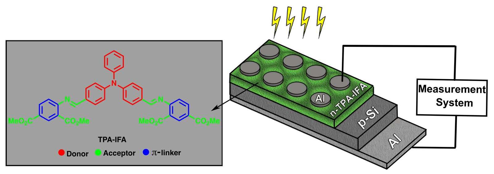
Silicon wafer with a 2-inch diameter p-type, orientation (100), 400 μm thickness, 1-10 ohm.cm was cut to suitable sizes with a diamond-tipped pen. First, the p-Si wafer was cleaned with acetone and methanol for 10 and 5 minutes, respectively an ultrasonic bath at 50°C. RCA1 and RCA2 procedures were used for p-Si wafer cleaning. H2O2:H2O solutions were prepared with a mixing ratio of 10:6. The RCA1 cleaning process was used to remove an organic layer; in this process, 5 ml of NH3 (%35) and 25 ml of H20 was mixed and heated to 70 o C. Then, 5 ml of H2O2:H2O solution was added to this solution. The Si substrate was put in the solution and kept for 15 minutes. RCA2 process was used to remove an inorganic layer; for this cleaning process, 5 ml of HCl (%27) and 25 ml H2O were mixed and heated to 70° C. Then 5 ml of H2O2:H2O solution was added to this solution. The Si substrate was put in the solution and kept for 15 minutes. To remove the oxide layer, the Si wafer was placed in a 2% HF solution for 3 minutes. Then it was rinsed with H2O. The Al ohmic contact was deposited with the help of a tungsten crucible under 10-6 bar pressure with a thermal evaporation system for the p-Si wafer. After, the Si wafer was annealed for five minutes at 570 °C in a pure argon atmosphere. Also, a soda-lime glass substrate was cleaned with chloroform, deionized water, methyl alcohol, acetone, and propanol for 10 minutes in an ultrasonic bath for the Hall measurement. 40 mg TPA-IFA was dissolved in 10 ml N,N-Dimethylformamide (DMF), and the solution was mixed for 10 minutes on a magnetic stirrer. A yellowish-clear solution was obtained. TPA-IFA solution was grown on the p-Si wafer and glass substrate by using the spin-coating method at 1000 rpm for 30 seconds. 1.15 mm diameter Al dots contacts were deposited with the same conditions as ohmic contact with a thermal evaporation system for p-Si wafer for electrical I-V measurements (Fig. 1). The samples grown on a glass substrate for Hall measurement were cut into a square of 7 mm by 7 mm, and their contacts were done from each corner with the help of silver paste.

Fig. 1. Schematic diagram of n-TPA-IFA/p-Si heterojunction diode
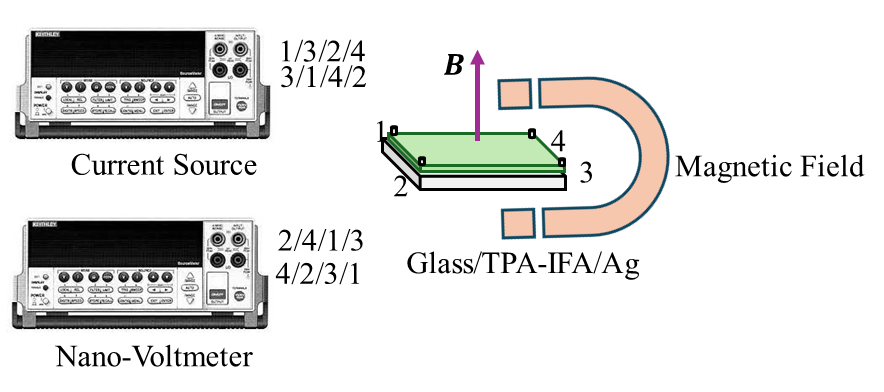
Current-voltage measurements were taken between -3V and +3V step by 0.01V at dark and under different light illumination conditions such as 20 mW.cm-2 , 40 mW.cm-2 , 60 mW.cm-2 , 80 mW.cm-2 , and 100 mW.cm-2 . Hall measurements were taken by van der Pauw technique at 0.5 T magnetic field between 100K and 400K step by 50K (Fig. 2).

Fig. 2 Schematic diagram of Hall measurements
3. Results and discussion
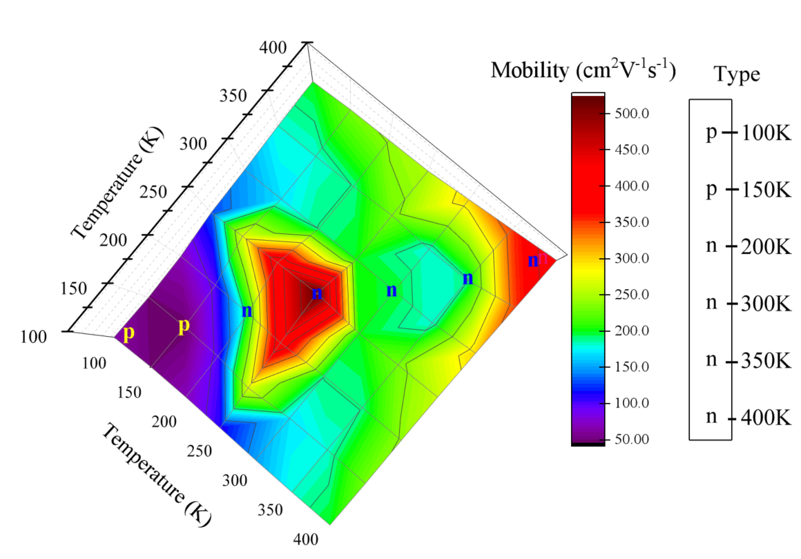
Fig. 5 shows a color mapping plot of mobility for TPA-IFA. Hall measurements were taken at 0.5 T magnetic field between 100K and 400K step by 50K. The sample showed p-type characterization at 100K and 150 K, while it showed n-type characterization between 200 K and 400 K. The carrier charge density type of the sample changed between 150K and 200K. The mobility of TPA-IFA varied depending on temperature. The mobility increased with increasing temperature between 100K and 250 K. Then it is decreased for 300K and 350K. Last, it increased to 400K. The temperature with the highest mobility value is 250K. According to these results, the TPA-IFA sample shows n-type behavior at room temperature.

Fig. 5 Results of hall measurement of the TPA-IFA thin film.
The produced n-TPA-IFA/p-Si photodetector's predicted LDR values increase from 10.15 to 18.84 dB when light intensity is raised from 20 to 100 mW/cm2 . LDR is essential because image sensors must function over various intensities. For example, if the LDR is sufficiently wide, a clear picture can be created in any situation. LDR values rise as the light intensity rises. Considering the findings, the n-TPA-IFA/p-Si heterojunction diode can be used as an image sensors and photo-devices. LDR values depending on light intensity are also given in Table 3.
4. Conclusions
In conclusion, we report for the first-time n-type TPA-IFA ("D-A-π-A") compound, in which triphenylamine is used as a donor, C=N imine part is an acceptor, benzene is a π-spacer, and ester is an acceptor/anchor. Also, The HOMO and LUMO energies of the TPA-IFA were calculated by DFT/B3LYP/6-311G(d,p) method using Gaussian 09 W. The hall measurements showed that the TPA-IFA sample shows n-type behavior at room temperature. Then, the spin coating method was used to create a heterojunction device based on an n-type TPAIFA thin film on the p-type Si substrate. We investigated the photodiode and photodetector parameters of the nTPA-IFA/p-Si heterojunction diode in both dark and different light conditions, considering its possible optoelectronic applications.
The n-TPA-IFA/p-Si heterojunction diode's ideality factor and Schottky barrier height were found to be, respectively, 0.716 eV and 3.01 in the dark and 0.755 eV and 1.63 in the 100 mW/cm2 . In this phenomenon, the ideality factor decreases as the Schottky barrier height increases with increasing light intensity. A heterojunction with a high rectification ratio of 104 and a low series resistance of 49 Ω was produced. Its lower series resistance value demonstrates the heterostructure's capability for effective photovoltaic cells. A large rectification ratio is seen for heterostructure contact. A decrease in tunneling resistance and space charge modulation across the interface may be the reason for enhanced electrical properties of heterostructures, such as an increase in barrier height and an ideality factor that deviates from unity.
下一篇: 硅孔光学元件