Abstract
Silicon Pore Optics (SPO) uses commercially available monocrystalline double-sided superpolished silicon wafers as a basis to produce mirrors that form lightweight high-resolution X-ray optics. The technology has been invented by cosine Measurement Systems and the European Space Agency (ESA) and developed together with scientific and industrial partners to mass production levels. It leverages techniques and processes developed over decades by the semiconductor industry to handle, process, and clean silicon wafers and plates. SPO is an enabling technology for large space-borne X-ray telescopes such as Athena and ARCUS, operating in the 0.2 to 12 keV band, with angular resolution aiming for 5 arc seconds. SPO has also shown to be a versatile technology that can be further developed for gamma-ray optics, medical applications and for material research.
2 Introduction
The launch of the high-energy astrophysics observatories XMM-Newton and Chandra in 1999 marked the culmination of two major optics development efforts, and made observations of the X-ray sky with unprecedented sensitivity possible. Significant investments were required, and two different optics technologies had to be developed to make these missions possible. The optics of XMM-Newton are based on electro-formed nickel, replicated from precision mandrels. They maximise effective area to make highresolution spectroscopy of distant sources possible . The Chandra optics, on the other hand, optimise the angular resolution at the cost of mass and effective area to provide high-resolution imaging. After more than two decades of active operations, these two missions remain in high demand for their stand-alone capabilities and the synergies with observations at other wavelengths. Their systems are however ageing, and the need for higher performance continues to increase.
The next generation high-energy astrophysics observatory will have to reach deeper into the Universe, keeping pace with the present and future ground and space based observatories like the James Webb Space Telescope (JWST), the Square Kilometer Array (SKA), and the Extremely Large Telescope (ELT). More photons will have to be collected from very distant sources, requiring larger effective area, good angular resolution to avoid source confusion, and more sophisticated detector instruments.
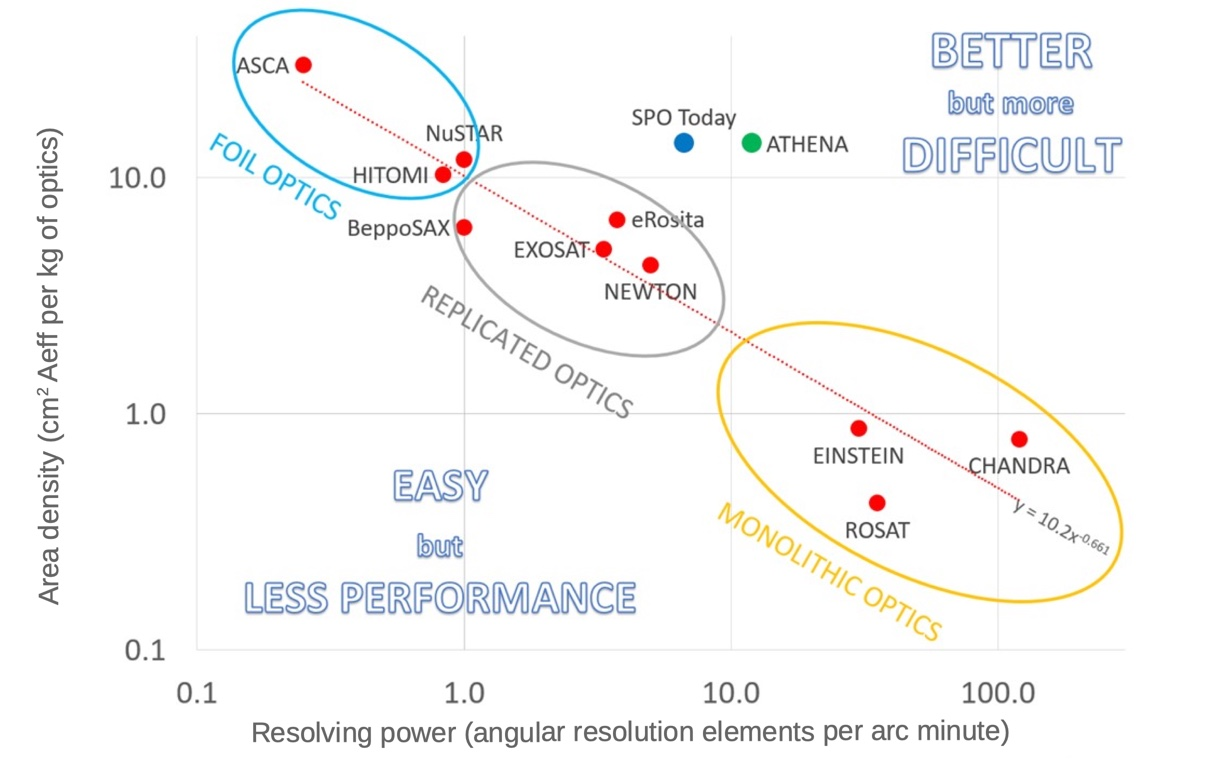
In Figure 1 the optics of these missions are compared, considering the aforementioned three parameters. The area density of the respective optics, expressed as effective area per mass of the optics is plotted against the resolving power of the optics, expressed as angular resolution elements per arcminute. A clear correlation is observed despite the fact that the optics technologies are very different, ranging from foil-based optics to replicated optics and monolithic optics. Each of these systems was developed and built with large effort, and each represents a major achievement, but they all follow a power law correlation. Even the Chandra optics, which are the result of extraordinary efforts in engineering and funding, manage to move only very slightly to the upper right side of the correlation line. The same is true for eRosita, which represents the highly optimised third generation of electroformed nickel technology.

Fig. 1
The graph illustrates that lightweight optics with large effective area but lower angular resolution, or high resolution but heavy optics with a limited effective area have been built until now. Current optics-making technologies have so far allowed for the production of systems where only two of the three parameters can be effectively optimized at one time. The optics for the Athena mission (green dot in Figure 1) however require a technological change to move away from this empirical power law into the ‘difficult corner’ to the upper right of the graph. Linear extrapolation of all the X-ray missions flown to date using the three previous conventional technologies suggests that it would be possible to deliver the resolution and effective area, but it would require a mass of about 7000 kg, which is the mass of the complete Athena mission. Or it could respect the mass allocation of 1000 kg and deliver the effective area, but with a severely degraded angular resolution of about 1.6 arcminutes.
3 SPO concept
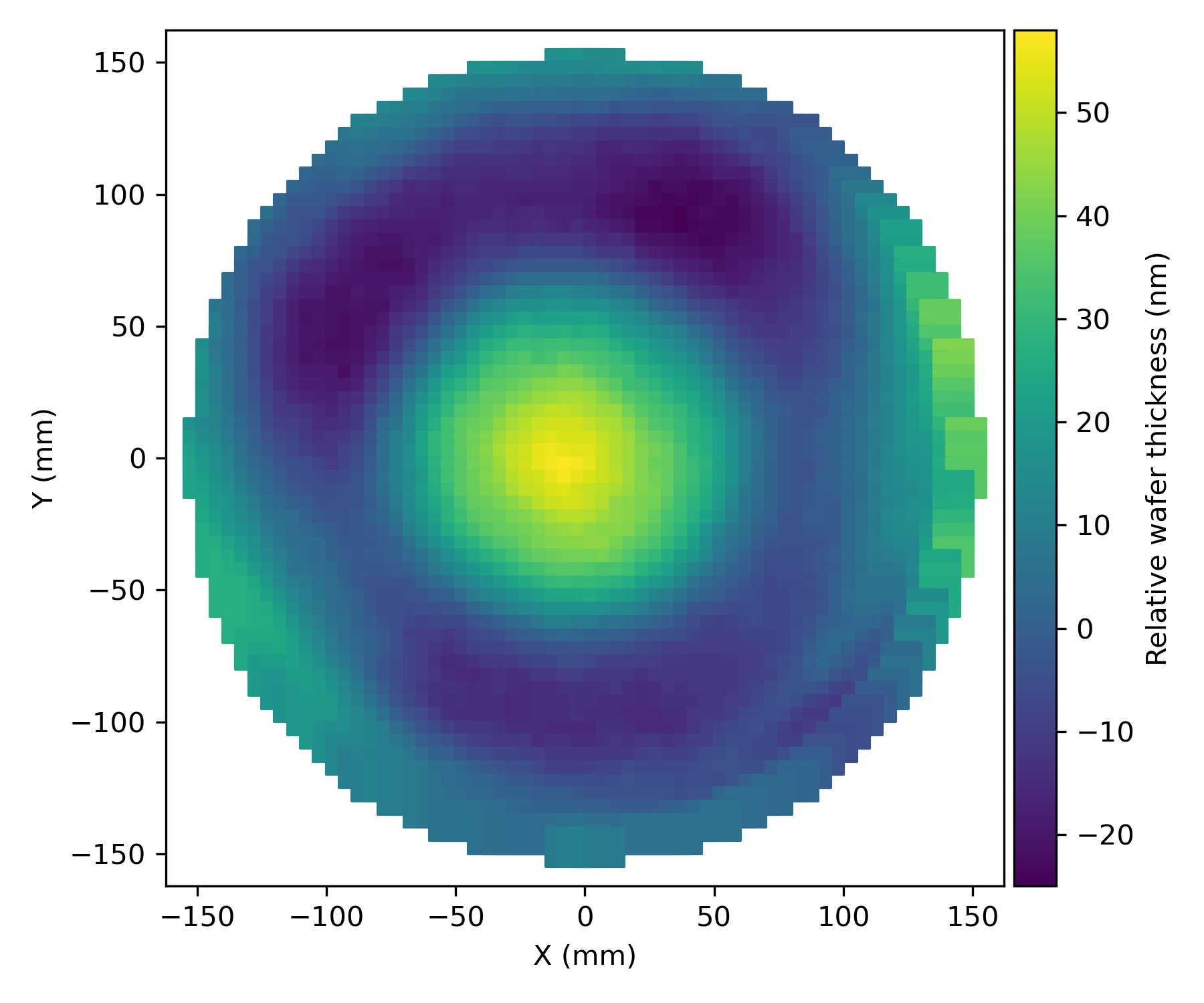
SPO development leverages the massive investments done in the semiconductor and automotive industries, which made available high-performance equipment, tools, materials and processes allowing highquality mass production. The work-horse of the semi-conductor industry are thin 300-mm wafers sawn out of monocrystalline ingots, grown from poly-crystalline silicon using the Czochralski method. These wafers are produced with outstanding quality for a modest cost: prime grade double-sided super-polished monocrystalline 300 mm silicon wafers have specifications of 0.1 nm root mean square (RMS) surface roughness and total thickness variation (TTV) of less than 0.2 µm (see Figure 2).

Fig. 2: Typical relative thickness map of a silicon wafer for SPO plate production. The data is plotted relative to the median thickness of 775110 nm of the wafer. The thickness is measured by Fizeau interferometry. Credit: cosine.
The plates are bonded on top of each other thanks to direct silicon bonding, which requires no adhesives. Starting from a mandrel that defines the optical design, plates are stacked and the mandrel figure is preserved owing to the plan-planarity of the mirror plates and the lack of any adhesive between plates. It results from the process a self-supporting stack of elastically deformed mirror plates that reproduce the shape of the mandrel. In such a stack, X-ray photons enter pores at low-grazing angles, are reflected on the reflective side of each plate, and exit the optics at the opposite end. These stacks consistute lightweight, moderate-to-high resolution, X-ray optics (see Figure 3).
The SPO mirror plates feature a patterned coating on their reflective side in order to enable direct silicon bonding (see Section 4.4). The patterning of the coating is performed via optical lithography. This process, sketched in Figure 5, consists of the following steps. Firstly, a photosensitive polymer is deposited on the reflective side of the SPO mirror plate. In a second step, a patterned photoresist layer is created by exposing the photosensitive polymer to ultraviolet light and developing it by immersing the sample in a chemical solution. Subsequently, an X-ray reflective coating is deposited using a sputtering deposition technique. Finally, chemical lift-off is performed to remove the coated photoresist resulting in a patterned coated SPO mirror plate.

Fig. 5: Schematic of optical lithography for SPO mirror plate with patterned X-ray reflective coating. Credit: cosine.
The plates are stacked in a concave mandrel, starting with a plate placed with the reflective side in contact with the mandrel and ribs pointing inwards, called the base plate. The mandrel is polished with the design shape of the stack. It can be cylindrical or conical, and can feature additional meridional curvature. The next plate is then brought into a similar shape as the base plate by using a ’die’, a tool with the same figure as the mandrel. The plate is attached with the mirror surface to the die, resulting in the ribs pointing outwards. The two plates are brought into close contact such that the two sets of ribs make contact and that direct bonding starts. In that moment, the plate copies the shape of the mandrel. This is the first reflective plate of the stack. The die then releases the plate and the process can be repeated, with the only difference being that the next plates are bonded with their ribs to the mirror surface of the upper plate in the stack. At the end of the process the stack is released from the mandrel and keeps the desired shape through the acting bond forces and the stiffening effect of the ribs.
The process repeats until the desired stack height is reached. Stacks up to 70 plates have been manufactured, 35 plates being the most common so far. Once the stack is finished, it is released from the mandrel and a final inspection is performed to measure the outer geometry and to visually check for defects. Prior to stacking, the mandrel axis is aligned with the die axis. The plate gripper, which is the reference for the plates alignment, is also aligned with respect to the die and mandrel. A robot is configured for one specific set of stacks defined by its mandrels and plate types. The robot needs to be reconfigured to produce stacks of different radii, plate geometry or figure.
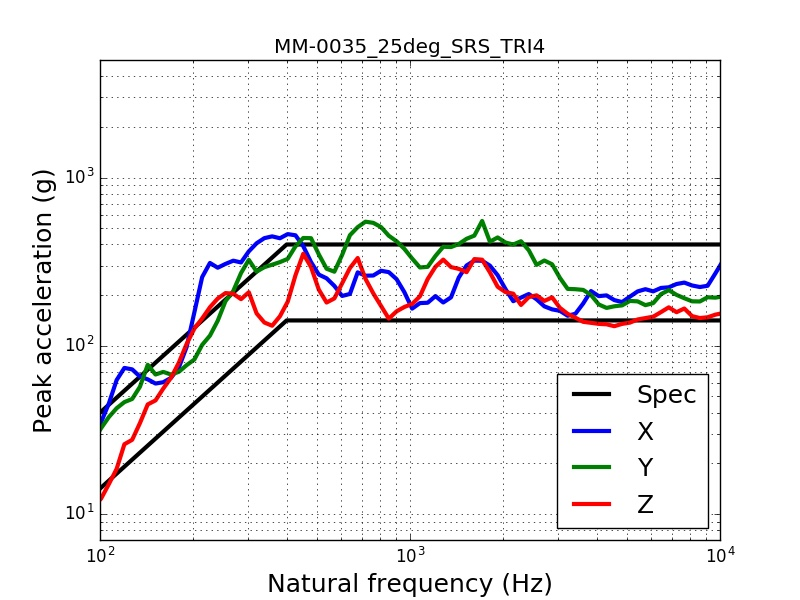
Mechanical shims are used to preload the DP flexures similarly to the vibration test. There, the preloading and SRS level simulate mirror structure distortions during one of the most dramatic event of the launch sequence as seen by the payload corresponding to the the release of the launch locks that will hold the mirror assembly during launch and are release once in space (shown in Figure 22). Figure 12 displays a SRS as measured on the test mount (also called input SRS) of a MM. Note that the SRS is isotropic, enabling the testing of all three axis in a single shock. Two high-speed cameras, each looking at one side along the optical axis, are used to assist in identifying failures, as well as their modes. Resonance searches are also performed to check on the structural integrity of the MM.

Fig. 12
A global quality indicator of the properties of the reflecting surface is derived by superimposing all the reflected images on their barycenters and calculating the half energy width (HEW) of the resulting image. This indicator is called the on centroid performance of the sample and is usually expressed in units of the HEW of the direct beam, and it represents the average surface quality on length scales of the order of a few to several millimeters.
Creating the optics technology for Athena is a formidable task, being addressed in a holistic and structured approach. From the very beginning the performance requirements were considered together with the programmatic constraints, in particular time and cost to build the flight optics, and the compliance with the environmental conditions of launch and space operations. Modularisation and serial production are essential for the production of the Athena optics, given its size, and MMs are rugged by design. Even the first optics demonstrator had to be compatible with mass production requirements of hundreds of mirror modules and hundred thousand mirror plates.
It is already recognized that SPO can be applied to applications other than Wolter I optics for spaceborne telescopes. The technique of replication of a mandrel in stand alone stacks of mirror plates can be used for any medium to large series manufacturing of mirrors with pretty much any kind of figure. Whether all the plates are used as mirrors or only the top one is a matter of design. Kirckpatrick-Baez designs or lobster eyes could also be implemented using a similar process. SPO technology also has the potential to create advanced gamma-ray focusing elements via the use of diffraction in the volume of the crystalline plates.