The feld of integrated photonics has advanced rapidly due to wafer-scale fabrication, with integratedphotonics platforms and fabrication processes being demonstrated at both infrared and visible wavelengths. However, these demonstrations have primarily focused on fabrication processes on silicon substrates that result in rigid photonic wafers and chips, which limit the potential application spaces. There are many application areas that would beneft from mechanically-fexible integratedphotonics wafers, such as wearable healthcare monitors and pliable displays. Although there have been demonstrations of mechanically-fexible photonics fabrication, they have been limited to fabrication processes on the individual device or chip scale, which limits scalability. In this paper, we propose, develop, and experimentally characterize the frst 300-mm wafer-scale platform and fabrication process that results in mechanically-fexible photonic wafers and chips. First, we develop and describe the 300-mm wafer-scale CMOS-compatible fexible platform and fabrication process. Next, we experimentally demonstrate key optical functionality at visible wavelengths, including chip coupling, waveguide routing, and passive devices. Then, we perform a bend-durability study to characterize the mechanical fexibility of the photonic chips, demonstrating bending a single chip 2000 times down to a bend diameter of 0.5 inch with no degradation in the optical performance. Finally, we experimentally characterize polarization-rotation efects induced by bending the fexible photonic chips. This work will enable the feld of integrated photonics to advance into new application areas that require fexible photonic chips.
Te feld of integrated photonics has advanced rapidly due to wafer-scale fabrication, with integrated-photonics platforms and fabrication processes being demonstrated at both infrared wavelengths (with a focus on the driving application areas of LiDAR and communications ) and visible wavelengths (delving into emerging applications areas, such as displays, optogenetics, and quantum systems). However, these demonstrations have primarily focused on fabrication processes on silicon substrates that result in rigid photonic wafers and chips, which limit the potential application spaces.
To date, there have been some prior demonstrations of mechanically-fexible photonics fabrication. One popular technique that has been used to achieve fexible photonics utilizes heterogeneous integration, where devices are initially fabricated on a rigid substrate and then transferred to a fexible substrate via either a directfip process or a stamp-assisted process. Another popular technique is monolithic integration, where devices are patterned directly on a fexible substrate that is temporarily supported by a rigid substrate. However, these prior fexible photonics demonstrations have been limited to fabrication processes on the individual device or chip scale, which limits scalability.
Results
Wafer‑scale fabrication process
Te fexible-wafer platform and CMOS-compatible 300-mm wafer-scale integrated-photonics fabrication process were developed at the New York Center for Research, Economic Advancement, Technology, Engineering, and Science’s (NY CREATES) Albany NanoTech Complex (the facility that houses AIM Photonics). All wafer-level processing was performed using NY CREATES’s suite of advanced 300-mm wafer processes for 193-nm immersion lithography, thin-flm chemical vapor deposition (CVD), reactive-ion etch (RIE), chemical-mechanical planarization (CMP), and wet cleaning in Albany, NY.
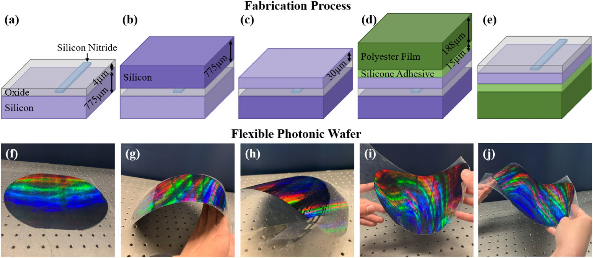
Te frst part of the process sequence is the fabrication of the photonic devices. Tese devices were fabricated on a 300-mm-diameter silicon wafer substrate covered with a 2-µm-thick tetraethylorthosilicate (TEOS) plasma enhanced chemical vapor deposition (PECVD) silicon-dioxide (SiO2) layer. Te thickness of this silicon-dioxide layer was measured to be 2.0±0.1 µm. A silicon-nitride (Si3N4) layer was then deposited on top of this silicondioxide thin flm using a PECVD process. Te thickness of this silicon-nitride flm as deposited was measured to be 180±6 nm. Both the silicon-dioxide and the silicon-nitride layers were deposited on industry-standard 300-mm CVD platforms. Tis deposited silicon-nitride flm was subsequently polished by a chemical-mechanical planarization (CMP) step in an advanced CMP tool, resulting in a smooth surface and a fnal layer thickness of 160±8 nm. Te silicon-nitride layer was then patterned using 193-nm immersion lithography and a dry-etch process on a 300-mm production etch system. As an example, for a designed waveguide width of 300 nm, the fabricated post-lithography width was measured to be 315 ± 5 nm, and the post-etch width was measured to be 300±10 nm at the top of the waveguide with a 2° taper on the waveguide sidewall that resulted in an 11 nm increase in the width at the bottom of the waveguide. Another TEOS PECVD SiO2 layer was then deposited on top of the Si3N4 layer, and its top surface was planarized back using another CMP step, leaving 2±0.1 µm of planarized SiO2 over the Si3N4 layer, as depicted in Fig. 1a. All of these process steps were performed at temperatures below 500 °C in order to minimize wafer bending due to flm stress induced by the thermal mismatch between the dielectric layers and the silicon wafer. Minimizing wafer bending was necessary because the subsequent wafer-thinning process (described below) is sensitive to wafer bow. A consequence of this thermal processing constraint was higher waveguide propagation loss for the silicon-nitride waveguides (discussed in detail in the following section).
Once the photonics stack was completed, a standard 300-mm-diameter silicon handle wafer was temporarily bonded to the top surface of the SiO2 layer in a 300-mm wafer bonder tool using an adhesive bonding material, as depicted in Fig. 1b. Ten, the bonded wafer pair was fipped over, and the original silicon substrate was ground down to 30±10 µm using a combination of course and fne grinding steps on a 300-mm grinder/polisher tool, as shown in Fig. 1c. Next, a 188-µm-thick polyester flm with a 15-µm-thick silicone adhesive layer was adhered to the top of the thinned silicon layer, as shown in Fig. 1d. Finally, the wafer was fipped back over, and the temporary silicon handle wafer was removed, as depicted in Fig. 1e. Photographs of the fabricated fexible integrated-photonics wafer are shown in Fig. 1f-j. Te photonic wafer was then diced into individual chips in the MIT.nano cleanroom for experimental testing.

Figure 1. Stack diagrams (not to scale) depicting process fow as (a) the silicon-dioxide and silicon-nitride layers are fabricated, (b) a temporary silicon handle wafer is bonded on top of the oxide, (c) the wafer is fipped and the silicon is thinned down, (d) a polyester flm is attached on top of the silicon layer, and (e) the wafer is fipped and the temporary silicon handle wafer is removed. Photographs of the fabricated fexible integratedphotonics wafer (f) fat, (g) convexly curved in one direction, (h) convexly curved in the other direction, (i) concavely curved, and (j) curved convexly and concavely simultaneously.
Optical characterization
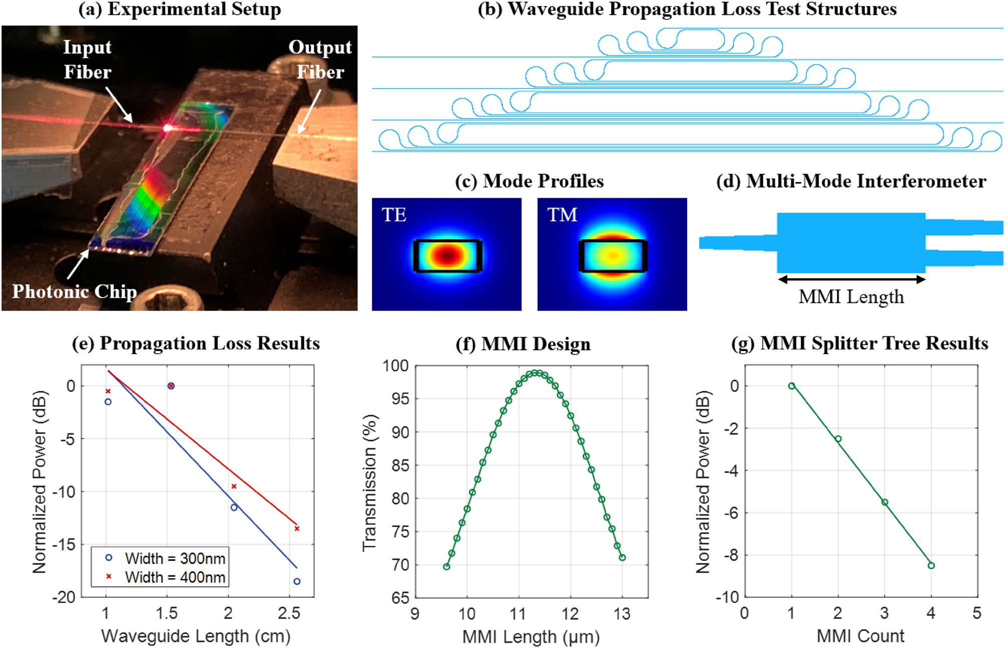
First, we experimentally demonstrated key optical functionality, including chip coupling, waveguide routing, and passive devices. To experimentally characterize the fexible photonic chips, the output from a 632.8-nmwavelength helium-neon laser was coupled on the chip via a tapered fber-to-chip edge coupler and the output light was coupled of chip via another edge coupler to a fber that was routed to a power meter, as shown in Fig. 2a.

Figure 2.
Next, waveguide loss was experimentally characterized using a suite of paperclip loss test structures, which are comprised of sections of straight waveguides with curves to loop back the waveguide and build up more propagation length. One suite of test structures consists of four individual paperclip test structures with four varying waveguide lengths. Te paperclip test structures are designed such that each variant includes the same number of loop-back curves to negate the efect of any curved waveguide loss. A top-view diagram of a suite of paperclip test structures is shown in Fig. 2b. We fabricated and experimentally characterized two suites of paperclip test structures: one with a waveguide width of 300 nm and the second with a waveguide width of 400 nm. Tese two widths were selected because they do not support higher-order modes (example simulated fundamental transverse-electric and transverse-magnetic mode profles for the 400-nm-wide waveguide are shown in Fig. 2c). Te measured propagation losses for the 300-nm-wide and 400-nm-wide waveguides were 12.1 dB/cm and 9.4 dB/cm, respectively, as shown in Fig. 2e (with some uncertainty due to variability in the edge coupler loss as discussed above). Tese measured losses are expected given that the waveguide fabrication process did not include processing for line-edge-roughness optimization (we measured similar losses for waveguides fabricated in a traditional process on a silicon handle wafer).
Finally, to demonstrate a more complex device and characterize chip-scale fabrication variation, a four-stage splitter tree consisting of 1×2 multi-mode-interferometer (MMI) splitters was fabricated and experimentally measured. A top-view diagram of the MMI is shown in Fig. 2d. An MMI is a symmetric 1-to-2-waveguide splitter device based on self-imaging principles that is designed to evenly split the input light to two output ports40. During the design process, the MMI width was chosen to be 2.8 µm to support a few higher-order modes in the MMI region. Given the selected MMI width, the MMI length was then chosen to optimize transmission to the two output ports. Simulation results showing the transmission into the symmetric output mode versus MMI length is shown in Fig. 2f. A fnal MMI length of 11.3 µm was chosen to optimize transmission through the device. We then cascaded four of these MMIs together into a four-stage splitter tree test structure. Using this fabricated splitter tree, the splitting ratio for a single MMI was experimentally characterized and calculated to be 2.9 dB, as shown in Fig. 2g, closely matching the ratio expected from simulation.
Discussion
First, we developed and described the 300-mm wafer-scale CMOS-compatible fexible platform and fabrication process. Next, we experimentally demonstrated key optical functionality at visible wavelengths, including chip coupling, waveguide routing, and passive devices. We experimentally demonstrated fber-to-chip edge coupling with 8 dB/facet coupling loss, propagation losses for 300-nm-wide and 400-nm-wide waveguides of 12.1 dB/cm and 9.4 dB/cm, respectively, and a splitting ratio of 2.9 dB for 1×2 MMI splitters, all at an operating wavelength of 632.8 nm. Ten, we performed a bend-durability study to characterize the mechanical fexibility of the photonic chips. We demonstrated bending a single fexible photonic chip 2000 times around cylinders with diameters ranging from 2 inches to 0.5 inches, with no noticeable degradation in optical performance. Finally, we experimentally characterized polarization efects induced by bending the fexible photonic chips. We compared device performance of the fexible chip lying fat versus while the chip was bent around two cylinders with varying diameters, and we found that the polarization of the output light changed as the chip was bent.
In the future, we will both continue developing this wafer-scale fabrication process and perform further in-depth characterization of the resulting fexible photonic chips. First, we will introduce a wafer-level etched dicing trench to the platform to enable a smoother facet and lower-loss edge coupler. Second, we will explore the feasibility of performing an annealing step and switching to an LPCVD silicon nitride to further reduce the waveguide propagation loss. Tird, we will perform further in-depth numerical analysis and experimental characterization of the mechanical properties of the fexible photonic chips, including quantifying the Young’s modulus, elastic constants, and fracture strength. Fourth, we will numerically model the impact of strain on the optical properties of the waveguide, and we will compare these simulated results with experimental results for the polarization rotation due to bending. Fifh, we will explore the efects of bending the chip in the other direction, which we expect will have an impact on the polarization rotation due to diferences in the stress and strain imparted on the waveguides. Sixth, we will develop a setup to perform automated bend testing to enable rigorous high-throughput characterization of the chip durability. Seventh, we will design more tailored photonic devices to further investigate the efects of chip bending on polarization and loss.
上一篇: 硅孔光学元件