ABSTRACT
Precise control of functionalization and etching have been required for surface modification and device fabrication of two-dimensional (2D) materials. Specifically, fluorination of graphene has been used to control the properties of graphene. Recently, xenon difluoride (XeF2) has been used for selective fluorination of graphene and etching of other 2D materials, such as hexagonal boron nitride (hBN) and transition metal dichalcogenides (TMDs). However, there is a lack of studies on key factors that govern the XeF2 treatment, which results in inconsistent behaviors of fluorination and etching. Here, we report control over chemical reactions between XeF2 and 2D materials using a chemical mediator of Si. Even a small amount of Si can accelerate the dissociation of XeF2, leading to the formation of chemically reactive xenon fluoride (XeF) that enhances the fluorination and etching of 2D materials. Additionally, our findings show that defects in 2D materials serve as chemically unstable sites that facilitate the additional dissociation of XeF2, generating F single atoms that easily form covalent bonds on the surface of 2D materials. Our study suggests that Si can be utilized as a reaction mediator to regulate XeF2 treatment on 2D materials, which has important implications for the fabrication of 2D electronic devices.
1. Introduction
Chemical reactions on the surface of 2D materials are essential for the functionalization and etching required to modulate the properties and pattern of the 2D materials. Xenon difluoride (XeF2), widely used as an etchant for silicon (Si) in micro-electro-mechanical systems (MEMS) and nano-electro-mechanical systems (NEMS), is a promising reactive gas for the fluorination of graphene and etching of hexagonal boron nitride (hBN) because the vigorous chemical reaction between XeF2 and 2D materials is possible in a scalable and intuitive way without heat or plasma. Moreover, the high etching resistance of graphene to XeF2 enables to use the ultrathin graphene as an etch stop mask in van der Waals (vdW) heterostructure devices. Utilizing this atomically thin graphene etch stop mask, various types of vdW heterostructurebased electronic devices can be realized, such as a vertically stacked complementary inverter that requires only half the space of conventional ones. Three-dimensional (3D) integration of such devices is a promising strategy to achieve the high-density integration required for modern electronic devices. In addition, complete fluorination of graphene opens up the band gap of the fluorinated graphene (FG) up to 2.93 eV, and this band gap engineering enables the electrical properties of graphene to be tuned, allowing it to be used as a versatile electronic material for nanoscale electronics. However, previous studies have exhibited inconsistent behaviors in terms of fluorination and etching due to a lack of research on the crucial factors governing the reactions between XeF2 and 2D materials. For example, it is difficult to fully fluorinate graphene up to the theoretical limit even at highpressure of XeF2 gas, even though it was demonstrated that the diamane, fluorinated bilayer graphene with diamond-like structure, can be produced by highly elongated exposure to high-pressure XeF2 . Meanwhile, it has been reported that significant fluorination of graphene can be achieved even at relatively low pressure of XeF2 gas and for short exposure times.
2. Experimental details
The first-principles electronic structure calculations were used by pseudopotentials and a plane-wave basis set within the density functional theory (DFT) . The ionic pseudopotentials were described using projector augmented wave (PAW) potentials implemented in Vienna Ab initio Simulation Packages (VASP). The energy cutoff for the plane-wave basis was set to 400 eV. The generalized gradient approximation (GGA) was used for the exchange–correlation potential . Geometries were optimized until the Hellmann-Feynman forces acting on the atoms became smaller than 0.03 eV/A. To account for weak van der Waals (vdW) interaction between graphene (or hBN) and adsorbates such as XeF2, XeF, SiF4, and F atoms, we adopted the DFT-D3 method of Grimme based on a semi-empirical GGA-type theory. We used 9 × 9 × 1 k-point sampling for atomic optimizations of graphene and hBN sheets with adsorbates. Furthermore, we carried out ab initio molecular dynamics (AIMD) simulations using the Nose-Hoover method in VASP. The simulations were performed at a finite temperature of approximately 300 K to observe the dynamic behaviors via the interactions between the adsorbates and graphene or h-BN sheets.
3. Results and discussion
There has been inconsistency in the fluorination or etching of 2D materials by XeF2 exposure. For example, it is difficult to fully fluorinate graphene up to the theoretical limit even at high-pressure of XeF2 gas, even though it was demonstrated that the diamane, fluorinated bilayer graphene with diamond-like structure, can be produced by highly elongated exposure to high-pressure XeF2. Meanwhile, it has been reported that significant fluorination of graphene can be achieved even at relatively low pressure of XeF2 gas and for short exposure times. While exploring the inconsistency in the fluorination or etching 2D materials by XeF2 exposure, we encountered that fluorination of exfoliated graphene flakes is influenced by the used substrates. Therefore, to unveil the effect of Si, which is commonly used as a substrate, on the chemical reactions of 2D materials with XeF2, we prepared mechanically exfoliated samples of monolayer graphene and multilayer hBN on the SiO2/Si substrates, which enabled to clearly observe the exfoliated samples due to large contrast. We attached the polymer adhesion to the side of SiO2/Si substrates to prevent the reaction of XeF2 gas with Si (see more details in Fig. S1). Then, we examined the fluorination behaviors of graphene samples in the presence or absence of an adjacent Si chip, which are referred to as the Si-assisted and Si-free conditions, respectively. We confirmed that the SiO2 has an ignorable reaction with XeF2 (Fig. S2), as reported elsewhere.
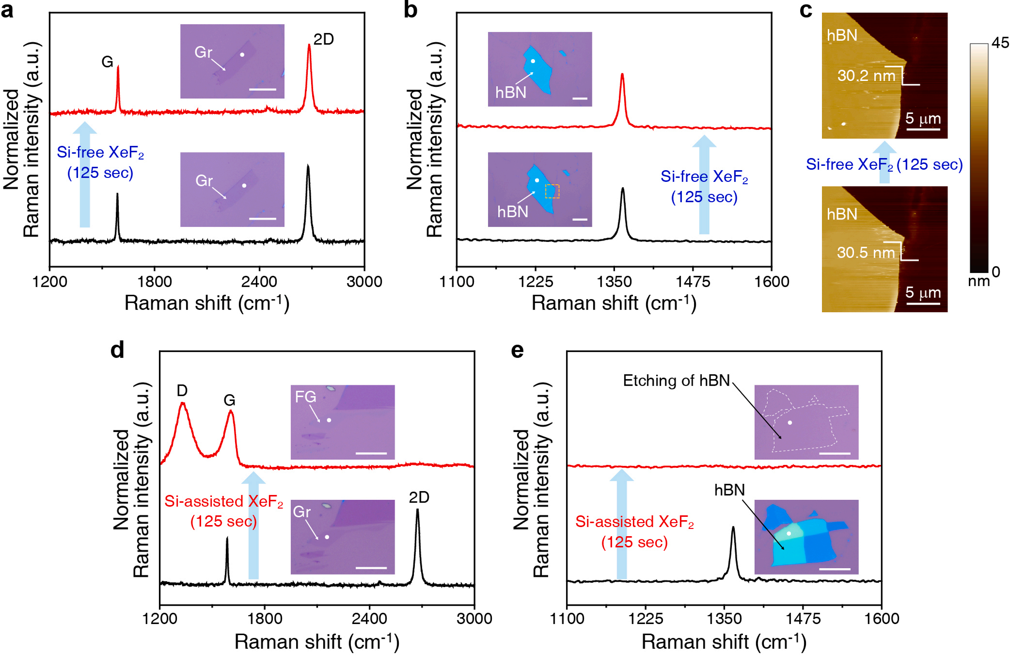
Fig. 1a,b show Raman spectra and optical microscopic images of the graphene and hBN before and after XeF2 exposure for 125 s under the Sifree condition. No significant change is observed in optical images and Raman signals. hBN also showed no change in the thickness and surface morphology as measured by AFM in Fig. 1c. This indicates that graphene and hBN have a negligible reaction with XeF2 under the Si-free condition, which agrees with our simulation result that the chemically stable XeF2 molecules have no interaction with graphene and hBN (Fig. S3 and Video S1).

Fig. 1. XeF2 treatment of 2D materials (graphene and hBN) in both Si-free and Si-assisted conditions. (a, b) Raman spectra and optical microscopic images of exfoliated monolayer graphene and exfoliated hBN before and after XeF2 treatment for 125 s in Si-free condition. (c) AFM images of hBN before and after XeF2 treatment for 125 s in Si-free condition. (d, e) Raman spectra and optical microscopic images of exfoliated monolayer graphene and exfoliated hBN before and after XeF2 treatment for 125 s in Si-assisted condition.
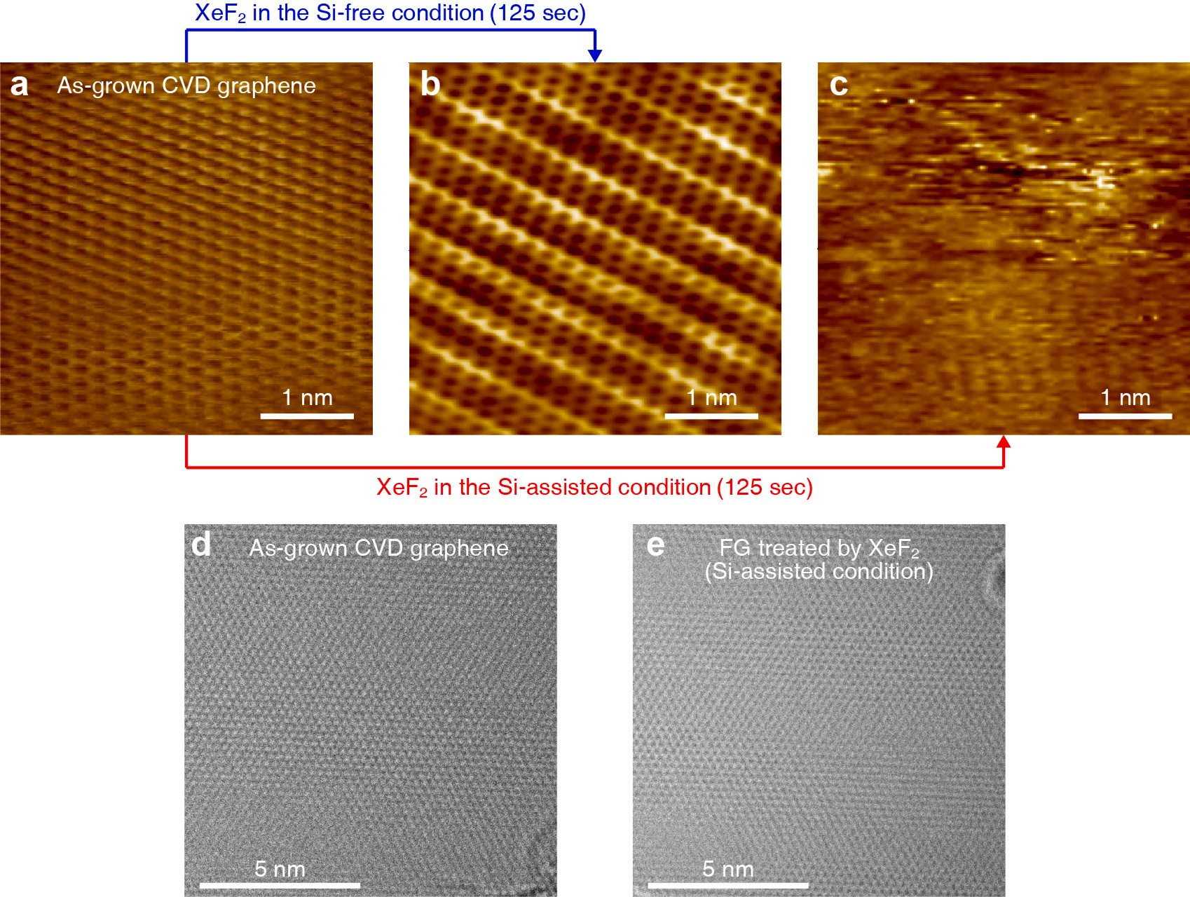
To obtain direct insights into the structural changes occurring in graphene during XeF2 treatment, we utilized STM and TEM analysis. These techniques allowed for a detailed examination of the morphology of graphene before and after fluorination. Given the benefits of using graphene with a large surface area for such measurements, we employed the graphene films synthesized on a Cu foil by chemical vapor deposition (CVD). The STM image in Fig. 2a displays the typical hexagonal structure of carbon atoms in the CVD-grown graphene before XeF2 exposure. Under the Si-free condition, the hexagonal structure of graphene remained unchanged even after XeF2 treatment, as shown in Fig. 2b, indicating no fluorination in the CVD-grown graphene. However, as shown in Fig. 2c, STM images of CVD graphene treated with XeF2 under the Si-assisted conditions show the absence of a hexagonal structure. This finding indicates that the properties of graphene were significantly altered by the XeF2 treatment under the Si-assisted condition. Based on the Raman spectra presented in Fig. 1d, the indistinct STM image observed under the Si-assisted condition was attributed to the conversion of graphene into FG. This conversion involves the attachment of fluorine atoms to the graphene surface, resulting in modified electronic properties and rendering the material insulating (Fig. S7). Although the hexagonal structure of carbon in the FG was not observed via STM analysis, TEM images clearly showed a distinct hexagonal structure for both as-grown graphene and FG under Si-assisted condition (Fig. 2d,e). This result highlights a significant advantage of the mild XeF2 treatment technique compared to other fluorination methods by a plasma that can damage the crystal structure of graphene. Note that the XeF2 treatment induces fluorination of graphene without the formation of defects, such as vacancies and holes. This non-destructive nature of XeF2 treatment is a noteworthy advantage.

Fig. 2. The analysis of the atomic structure of graphene. (a, b, c) The STM images of as-grown CVD graphene, XeF2-treated CVD graphene (for 125 s) under the Sifree condition, and XeF2-treated CVD graphene (for 125 s) under the Si-assisted condition. (d, e) The TEM images of as-grown CVD graphene and FG treated by XeF2 under the Si-assisted condition.
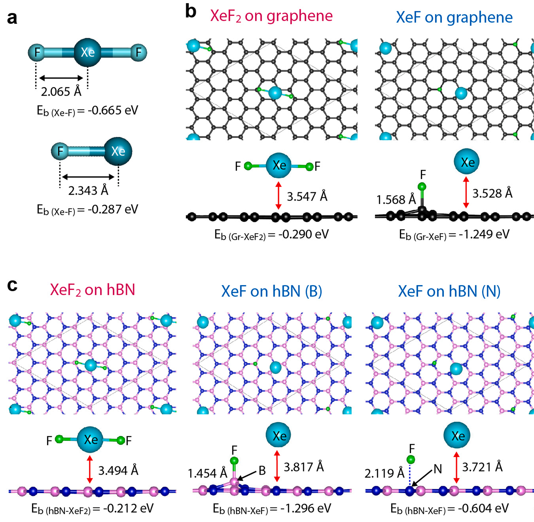
As an initial step, we calculated the Xe − F binding energy (Eb (Xe− F)) for both XeF2 and XeF molecules to assess their feasibility of releasing F upon reaction with the target material (see more details in Experimental Section). As shown in Fig. 3a, the calculated Eb (Xe− F) in XeF2 is − 0.665 eV, which is lower than that for XeF (− 0.287 eV). A lower value of Eb signifies a stronger bond, leading to a shorter Xe − F bond length in XeF2 compared to XeF. These results indicate that XeF has smaller chemical stability than XeF2. Thus, the XeF is more likely to be dissociated into Xe and F atoms and has a low tendency to retain fluoride content. Subsequently, we compared the chemical reactions of XeF2 and XeF with 2D materials, as shown in Fig. 3b,c. In case of graphene (Fig. 3b), the XeF2 shows non-dissociative adsorption on the graphene surface with a weak van der Waals (vdW) interaction (Eb(Gr− XeF2) = − 0.290 eV). The weakly adsorbed XeF2 on the graphene surface dopes the graphene, which is in agreement with our electrical measurements (Fig. S10). In contrast, the XeF exhibits an energetically favorable tendency to fluorinate the graphene by delivering an F atom to the graphene surface (Eb(Gr− XeF) = − 1.249 eV). This supports the fluorination of graphene with a stable configuration of C-F bonds, enabling to use of graphene as an etch stop layer. Similar to the case of graphene, the XeF2 exhibits a weak vdW interaction with the hBN (Eb(hBN− XeF2) = − 0.212 eV) without chemical dissociation (Fig. 3c), while the XeF displays high reactivity with the hBN, leading to the chemisorption of F atoms on the hBN surface with large binding energies (− 1.296 eV for B − F bond and − 0.604 eV for N − F bond). The XeF generated from dissociation of XeF2 through Si accelerates chemical reaction of 2D materials. Therefore, we might speculate that graphene and hBN surfaces are fluorinated due to the presence of XeF under the Si-assisted condition.

Fig. 3. Simulation results comparing the chemical reactivity of XeF2 and XeF towards 2D materials. (a) The calculated molecular structures describing the bonding length and bonding energy of both XeF2 and XeF. (b, c) Simulation results comparing the chemical reactions of XeF2 and XeF with graphene and hBN.
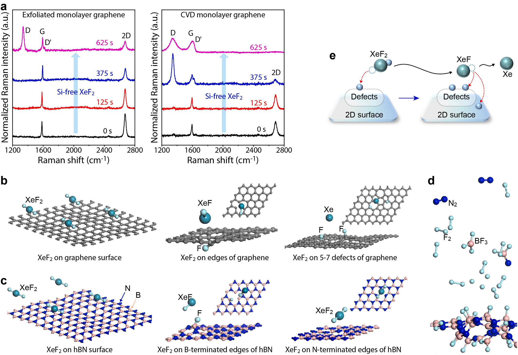
To provide a detailed explanation of the hBN etching process, we considered a situation in which the hBN sheet region with N vacancy is covered with F atoms resulting from the dissociation of XeF2 or XeF. The etching process in such an F-rich situation is simulated using AIMD, of which the results are provided in Video S2. A variety of reaction products can be generated during the etching process of fluorinated hBN sheets, including BF3, NF3, N2, and F2. To investigate the formation of these products, we have calculated the binding energies per atom for each molecules using DFT calculations (Table S1). Based on DFT calculations results, it becomes evident that the ease of binding follows the order BF3 > N2 > NF3 > F2. From the AIMD calculations, BF3 molecules are formed along with N2 and F2 molecules formation around the B-terminated vacancy edges of hBN. The AIMD calculations did not yield NF3, however, the presence of sufficient nitrogen atoms during the etching process could lead to the formation of NF3 molecules. A snapshot of the etching process is depicted in Fig. 4d, where the BF3 and N2 molecules are noticeable (see the red circles), with many B-F bonds on the hBN sheet. Compared to the speculation related to the fluorination of the pristine hBN given in the previous paragraph, we found that the etching occurs by the F atoms, destroying the defective hBN sheet by forming BF3 and N2 molecules. Thus, our AIMD simulation results support the etching process that prefers over the fluorination on the hBN sheet. Indeed, our AIMD results, combined with DFT results in part, provide a comprehensive explanation for the experimental process related to fluorination and etching. Taken together, the dissociation of XeF2 from defects within the 2D material causes the formation of XeF, and this XeF then facilitates the fluorination process and the etching of the 2D material, as depicted in Fig. 4e.

Fig. 4. Enhanced fluorination by XeF2 of defective 2D materials. (a) Raman spectra of exfoliated graphene and CVD graphene treated with XeF2 under the Si-free condition for different treatment times. The CVD graphene with more defects shows enhanced fluorination compared to exfoliated graphene with less defects. (b, c) Simulated reaction at defect sites of graphene and hBN with XeF2 under the Si-free condition. XeF2 itself shows no chemical reaction with defect-free graphene. Meanwhile, the XeF2 is dissociated at the defect sites of graphene, providing a fluorine atom even under the Si-free condition. In case of hBN, the XeF2 is dissociated only at the B-terminated defect sites. (d) Snapshot of the etching process obtained in the AIMD simulation. (e) Schematic illustration for the chemical reaction between XeF2 and defect sites of 2D materials under the Si-free condition.
4. Conclusions
Our study elucidates the chemical reaction mechanism between XeF2 and 2D materials, like graphene and hBN, through experimental analyses and computational simulations. We verify that the Si acts as a chemical mediator to facilitate the graphene fluorination and hBN etching during the XeF2 treatment. Thus, our work offers fundamental insights for understanding the chemical reaction between XeF2 and 2D materials and provides a clue to explain the inconsistent fluorination extent in the previous studies using XeF2. Our findings are crucial for the reproducibility and precise control of XeF2 treatment in 2D materials and open up an avenue for further exploration in the functionalization of 2D materials, intricate patterning techniques, and their utilization as electronic materials.