ABSTRACT
Defect inspection methods are basic steps in electronic chip manufacturing and power device production processes in the semiconductor industry. Based on stress induced photoelastic anisotropy, in-line polarized stress imaging (PSI) and quantitative determination of the local shear stress component are possible in single crystalline silicon wafers. Hereafter, such polarization stress images are compared and validated quantitatively with results of finite element simulations based on different 3D elastic models. Uniquely, high resolution at high throughputs is achieved for 300 mm wafer size in the present quantitative stress imaging study.
1. Introduction
Defect inspection methods are basic steps in electronic chip manufacturing and power device production processes of the semiconductor industry. Based on these methods, practically dislocation free Si wafers and epitaxial layers can be produced in various applications by sorting out defected areas or wafers and optimizing ion implantation and thermal treatment steps. Polarization imaging is widely accepted among such defect inspection methods because of its nondestructive nature based on the phenomenon of stress induced birefringence. Polarization imaging methods were used successfully to identify small defects, even single dislocations, in wide band gap semiconductor materials such as GaN , SiC , Ba(NO3)2 and diamond.
If section of the indicatrix with the plane normal to the light propagation is an ellipsis (indicated by yellow color in Fig. 1), birefringence produces phase delay (δ) between the polarization components of the light wave. Parameters of this ellipsis can be readily obtained as B* ijrirj = 1 by a projection of Bij into B* ij, if the light wave propagates along one axis of the coordinate system (e.g. along z axis as shown in Fig. 1).

Fig. 1. (a) Schematic image explaining light birefringence in Si. The blue ellipsoid is the indicatrix, with the principal axes of Bij (blue vectors). Intersection of the indicatrix with the normal plane of light wave is indicated by a yellow ellipsis. (b) Major and minor axes of the ellipsis and angle of the major axis (β) are also indicated in the x-y plane section for isotropic stress free Si (dashed line) and for stressed Si (solid line).
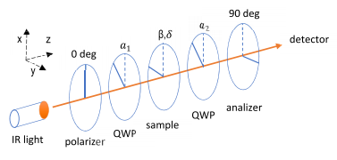
Polarization imaging can be carried out by a polariscope. Such a polariscope consists of mostly a polarizer, the sample and an analyzer plate. Additionally, quarter wave plates (QWP) are also placed between the sample and the different polarizer plates (named as general or circular polariscope) as shown in Fig. 2. If absorption of the sample and the different optical elements is neglected, the orientation of these optical elements together with the δ (phase difference) and the β (angle of the main axis of birefringence) determine the intensity ratio of the detector and the incident light (I/I0).

Fig. 2. Optical model of a general dark field polariscope with polarizer, two quarter wave plates (QWP), analyzer and the sample. Parameters of the optical elements are also indicated.
For the present polarization stress imaging, a 300 mm size 100 Si wafer, which was free from large defects, was used. The wafer was held by three grips, which were aligned approximately equal distances along the circumference of the wafer. One grip applied radial force (F) to the wafer in perpendicular direction to the [110] wafer notch, while the two other grips fixed the position of the wafer (see Fig. 3a). This geometry, in principle, is similar to the so called Brazilian test, which is used for photo-elastic calibration in the literature.
Polarization stress imaging was carried out using the PSI-3100 equipment with different F forces in the 0–0.7 N range. A couple of PSI images acquired by F––F0 (initial grip force) and F––F0+0.4 N (enhanced grip force) are shown in Fig. 3b and c, respectively. As seen, the radial forces along the perimeter produce strong patterns, which account for the stress induced birefringence in the Si wafer. Additionally, smaller stress lobes (right from the upper left and also right from the lower left grips), which account for internal defects along the wafer edge, are also visible in Fig. 3b and c. To tests the reproducibility of the imaging method the measurements were repeated several times (see Supplementary S1).

Fig. 3. a) Schematic of the edge gripped 300 mm diameter wafer with two fixed grips and one grip applying constant F force. Notch indicates the [110] direction for a (001) wafer plane (100 wafer). PSI images of a 100 wafer with grip force of b) F––F0 and c) F––F0+0.4 N.
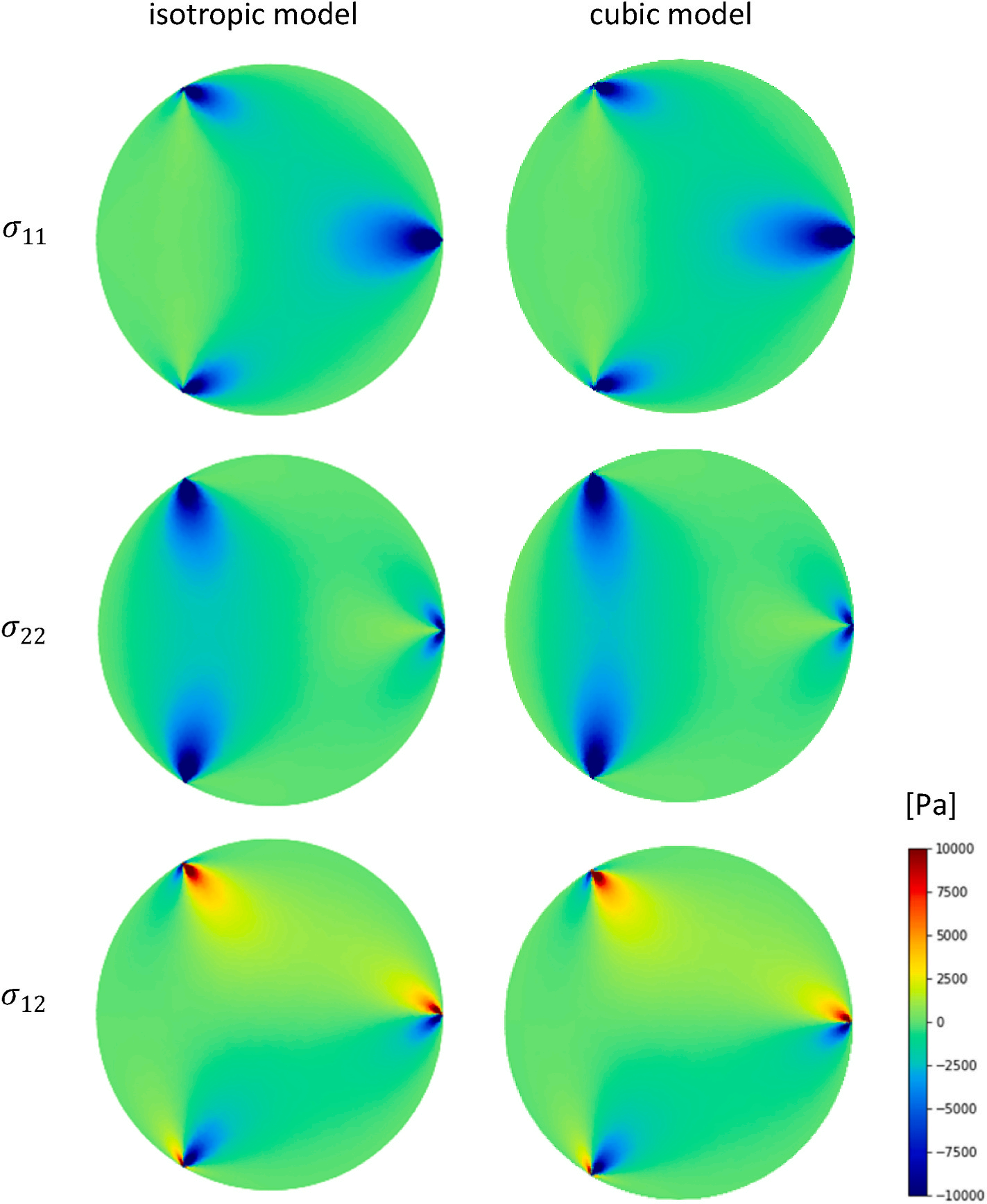
In the present work, results of an isotropic (Young modulus of E = 170 GPa and Poisson’s ratio of ν = 0.28) FE model and a cubic or anisotropic (C11 = 165.7 GPa, C12 = 63.9 GPa and C44 = 79.6 GPa) elastic FE model are presented. Further details on the FE modelling can be found in the Supplementary S2. To be conform with the PSI geometry and Equation (10), the z averaged in-plane stress components (σ11, σ22 and σ12) are shown in Fig. 4 for both models. Integration and part of the postprocessing was performed in python.

Fig. 4. In-plane σ11(x, y), σ22(x, y) and σ12(x, y) stress components obtained from FE simulations with isotropic and cubic models. Each stress components were averaged over the wafer thickness and were obtained from the same FE simulation with F = 0.4 N grip force.
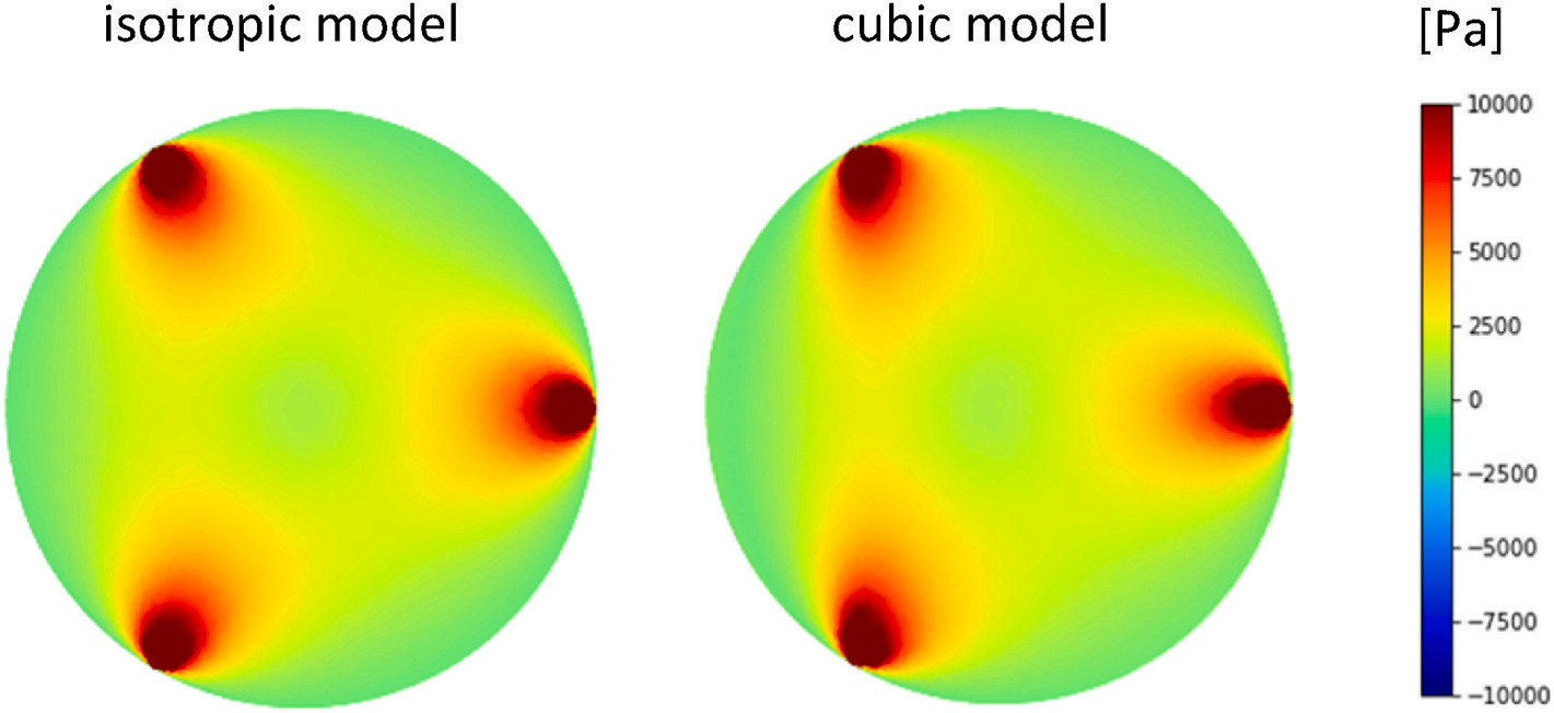
To validate the FE results and reveal the symmetric/asymmetric effect of the three grips in the isotropic/anisotropic cases, the von Mises stress component is also plotted for the two models in Fig. 5. The von Mises stress shows threefold symmetry and circular stress levels as it is anticipated from the theory of Hertzian contact for isotropic solids , while this symmetry is broken slightly in the cubic (anisotropic) Si wafer.

Fig. 5. The von Mises stress averaged over the wafer thickness as determined from the FE simulations for isotropic and cubic models with F = 0.4 N.
Conclusion
Common high throughput and high resolution stress imaging was performed in the present work using a special in-line polariscope. For comparison with similar stress imaging equipments, a quantitative measure for the information production was proposed. Stress patterns of an edge gripped 300 mm wafer was measured experimentally for different edge loads and compared to the results of Comsol finite element simulations. Quantitative comparison was made between the experimental and the simulation results and, accordingly, whole wafer polarized stress images with fine details on the shear stress distribution of individual defects were presented. For 100 Si wafers, analytical connection was proved between the stress field of the defects and their observed intensity distribution.
上一篇: 利用背面腔蚀刻对硅微环谐振器进行热优化