Abstract: We demonstrate the growth of 3C-SiC with reduced planar defects on a micro-scale compliant substrate. Heteroepitaxial growth of 3C-SiC on trenches with a width and separation of 2 µm, etched into a Si(001) substrate, is found to suppress defect propagation through the epilayer. Stacking faults and other planar defects are channeled away from the center of the patterned structures, which are rounded through the use of H2 annealing at 1100℃. Void formation between the columns of 3C-SiC growth acts as a termination point for defects, and coalescence of these columns into a continuous epilayer is promoted through the addition of HCl in the growth phase. The process of fabricating these compliant substrates utilizes standard processing techniques found within the semiconductor industry and is independent of the substrate orientation and offcut.
1. Introduction
Silicon carbide (SiC) is a wide-bandgap compound semiconductor with high electrical field breakdown and thermal conductivity, which makes it ideal for high-voltage power electronics and other applications in harsh environments. SiC can exist in a number of different crystalline forms due to the stacking sequence of the C-Si bilayers; these are known as polytypes. The hexagonal structured 4H-SiC is highly mature and is available as single crystal substrates, which when paired with high-temperature homoepitaxial growth, form the basis for commercially available power electronic devices. The cost of this material, however, both in terms of the starting substrate and epitaxy, is extremely high and limits its uptake in mass markets.
The cubic form of SiC (3C-SiC) has a zinc-blende (diamond) structure and stabilizes at lower temperatures than other polytypes, allowing it to be grown on silicon (Si). The heteroepitaxial growth of 3C-SiC offers many advantages such as low-cost, large-diameter and high-quality starting Si substrates as well as low epitaxial growth temperatures . 3C-SiC is of particular importance to power electronics in the 600–1200 V range, as it has a low built-in voltage, which accounts for the low specific on-resistance (Ron.sp) losses and large 3C-SiC/SiO2 barrier, which potentially support devices’ reliability.
2. Materials and Methods
Trenches of 2 µm width and 2 µm separation (defined as 4 µm pitch) were etched to a depth of approximately 4 µm into on-axis 100 mm diameter Si(001) substrates using UV photolithography and reactive ion etch (RIE) processing, with an SF6 and O2 plasma. The trenches were aligned to the <110> crystal plane directions. Photoresist was removed by solvent cleaning in acetone before being subjected to an RCA clean. The wafers were then loaded into an epitaxial reactor, ensuring no contamination was introduced into the growth system, and the substrate surface was primed for epitaxy.
Epitaxial growth and thermal annealing were performed within an LPE ACIS-M8 reduced-pressure chemical vapor deposition (RP-CVD) reactor at the University of Warwick. 3C-SiC films were grown at a temperature of 1325℃ using trichlorosilane (TCS, SiHCl3) and ethylene (C2H4) with a C/Si ratio of 1.4, within a H2 carrier gas at a growth rate of ~6 µm/h. A carbonization process was used to initiate the growth of the 3C-SiC, which involved the deposition of a thin seed layer using C2H4 at a temperature range starting at 900 ◦C and ramping up to 1140 ℃. On selected samples, the surface profile of the trench walls was modified using H2 annealing at 1100 ◦C for 10 min prior to a carbonization process.
3. Results
Dry etching of silicon can lead to unwanted features such as striations along trenchwalls and micro-trenches in the base of a trench due to limitations in UV photolithographyand imperfect dry etching processes. Annealing the trenches in Hz modifies theimperfect profile of the mesa walls, giving them a smooth surface, and thereby eliminatesthese features. Annealing at a sufficiently high temperature can facet and rund the surfacesof the Si mesas. Samples not exposed to this baking retain their flat (001)-orientation surfaceand base and {110} sidewalls (see Figure 1). In this study, the Hz annealing process wasfound to have a minimal effect on the trench depth, with the sample depths measured at4.2 um and 4.1 um before and after annealing, respectively.

Figure 1. Cross-sectional SEM micrographs highlighting the rounding of the Si trench profile beforeand after being subject to 1100 'C H2 annealing.
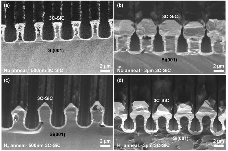
Conformal epitaxial growth of thin layers of 3C-SiC was found in the Si trenchesand on the sidewalls for thin epilayers; however, as the epilayer thickness increased, thesidewall growth was suppressed and voids formed within and above the trenches (seeFigure 2). We speculate that this was due to the shadowing effect of the epilayers growingon top of the structures, preventing the flow of precursors into the underlying trenches.Growth on the Si structures that were runded thrugh thermal annealing appeared moredisordered than on the unannealed structures and, in either case, no fusion of the separatedepilayers was observed at a growth thickness of 3 um.

Figure 2. Cross-sectional SEM micrographs of 500 nm and 3 um 3C-SiC heteroepitaxially grown on Sitrench structures without annealing (a,b) and after 1100°C H, annealing (c d).
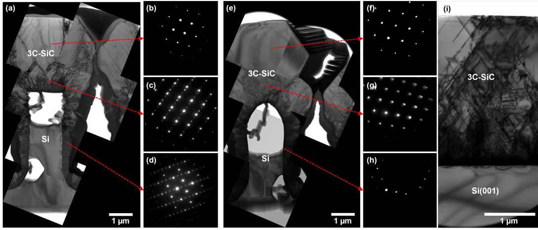
Cross-sectional TEM showed that the 3C-SiC grown on both rounded and non-rounded structures was crystalline; however, a clear difference in defect density could be observed between the samples (see Figure 3). The rounded surface of the annealed structure was observed to direct stacking faults away from the center of the peak, resulting in an almost defect-free region above the Si structure (see Figure 3e). The selective area electron diffraction (SAED) patterns showed that while the material close to the Si structure had elements of hexagonality caused by the high density of stacking faults within the epilayer, the 3C-SiC growing above the Si structure was monocrystalline in both cases. A clear interface could be observed between adjacent structures, showing that the layers had not coalesced, and, in both cases, the sides of the 3C-SiC growth columns were highly disordered.

Figure 3. Cross-sectional TE micrographs of 3 um 3C-SiC grown on Si trench sidewalls without(a) and with 1100°C H2 annealing (e). SAED patterns of 3C-SiC grown on both structures con firmthat the material above the sidewall profile is monocrystalline (b ,f) while 3C-SiC on the surfaces andsidewalls of the structures shows elements of polycrystallinity and defectiveness (c d,g,h). 3C-SiCgrown directly on a Si(001)substrate is shown in (i) for comparison.
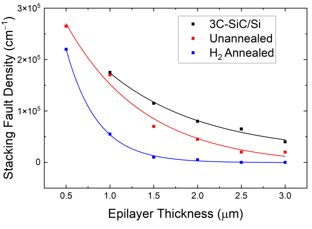
The stacking fault density in the region above the pillars of each sample was estimatedfrom 'TEM images and compared to that of the grwth on non-patterned Si (see Figure 4)The density of stacking faults, based on these local measurements, was found to decreasefor the patterned structures, with a further significant reduction after H, annealing throughthe channeling of planar defects away fmm the center of the mesa.

Figure 4. Linear stacking fault density calculated from TEM micrographs at varying depths. Thedensity of defects for patterned wafers is taken directly above the Si structures.
Improving Coalescence with HCl
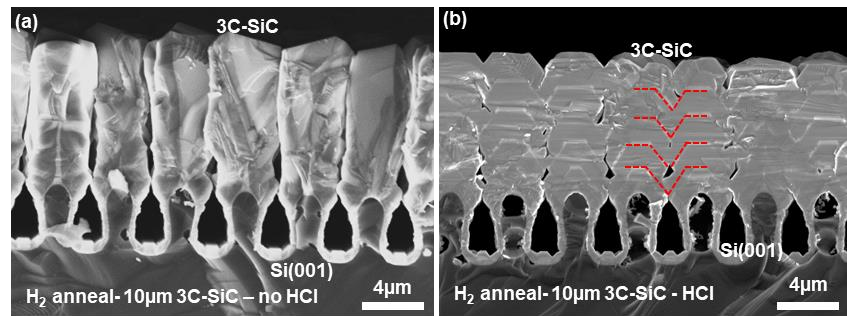
One key limitation of the method described so far is the inability of individual 3C-SiCcolumns to fuse with their neighbors and create a coherent epilayer. It has been proposedthat the lack of coalescence of these 3C-SiC films may be due to their thinness; howeverincreasing the growth of 3C-SiC to 10 um did not trigger any fusion. Instead, separateindividual columns of 3C-SiC grew upon each of the Si structures (see Figure 5a). In anotheridea, the disordered structure of 3C-SiC is thought to cause the lack of coalescence, and so 500 sccm of HCl was introduced into the growth process of 3C-SiC to assess the impact ofthis etching agent. At typical growth temperatures of 3C-SiC, HCl is found to etch highlydislocated regions of material faster than ordered crystal areas and, hence, can be used topromote the faceted growth of 3C-SiC. In the case of growth on Si(001), the additionof sufficient HCl increased the prevalence of the 3C(001) and 3C(111) surfaces. Whenthese regions met, they were observed to coalesce much more effectively (see Figure 5b)Al doping markers were grown in situ during the epitaxial growth of the 10 um 3C-SiCepilayer with additional HCl atevery 2 um of grwth to highlight the growth evolution ofthe film when observed by SEM. Even with the H, annealing process, the growth frontswere found to be the (001)and (111) crystal planes, and the length of (001) was found toincrease as the epilayer increased in thickness, indicating the fusion of the (111) planesWere this epilayer to be grown up to >10 um, a flat epilayer surface may be achieved, asthe (111) planes may fuse together entirely.

Figure 5. Cross-sectional SEM micrograph of 10 µm 3C-SiC grown on Si trench structures subject to 1100 °C H2 annealing without HCl (a) and with additional HCl (b) during epitaxy. The growth fronts of one column are highlighted in red to show the growth evolution.
Further optimization of this growth process is required to improve the coalescence of these columns and to improve the surface morphology of the layer. Increasing the flow of HCl will impact the prevalence on different 3C-SiC growth fronts; however, improvement could also be achieved by modifying the aspect ratio of the mesas and trench separation. Chemical mechanical polishing (CMP) could be employed to give a smooth top surface, making the material suitable for further epitaxy, wafer bonding or device fabrication, as well as producing a high density of voids at the 3C-SiC/Si interfaces on the patterned structures due to the increased Si surface.
The growth of 3C-SiC on patterned substrates leads to a reduction in the stacking faultdensity by trapping defects at the sidewalls of 3C-SiC columns. A further reduction indefect density is obtained by modifying the geometry of the Si structures, which can beachieved through thermal annealing in H2. Rounding the starting Si structure is shown togenerate planar defects, which propagate along the {111} crystal planes that direct awayfrom the [001] growth direction. Conformal epitaxial growth of 3C-SiC on such micro.structures begins to form on Si; however, once a thickness comparable to the separationbetween structures is obtained, growth within the trenches is suppressed and voids areformed. 'These voids act as natural defect temmination points and may help reduce thermallyinduced wafer bow by breaking up the continuous interface of 3C-SiC/Si.
上一篇: 高通量在线硅晶圆检测中的定量剪切应力成像
下一篇: 超薄锗独立膜的可持续生产