Abstract: Germanium (Ge) is a critical material for applications in space solar cells, integrated photonics, infrared imaging, sensing, and photodetectors. However, the corresponding cost and limited availability hinder its potential for widespread applications. However, using Ge freestanding membranes (FSMs) allows for a significant reduction in the material consumption during device fabrication while offering additional advantages such as lightweight and flexible form factor for novel applications. In this work, we present the Ge FSM production process involving sequential porous Ge (PGe) structure formation, Ge membrane epitaxial growth, detachment, substrate cleaning, and subsequent reuse. This process enables the fabrication of multiple high-quality monocrystalline Ge FSMs from the same substrate through efficient substrate reuse at a 100 mm wafer scale by a simple and low-cost chemical cleaning process. A uniform, high-quality PGe layer is produced on the entire recovered substrate. By circumventing the use of conventional high-cost chemical–mechanical polishing or even substantial chemical wet-etching, and by using an optimized PGe structure with reduced thickness, the developed process allows for both cost and an environmental impact reduction in Ge FSMs production, lowering the amount of Ge used per membrane fabrication. Moreover, this process employs large-scale compatible techniques paving the way for the sustainable production of group IV FSMs for next-generation flexible optoelectronics.
1. Introduction
Germanium (Ge) is at the forefront of many applications in optoelectronics and photonics including lasers, wave guides, photodetectors, THz transmission, thermophotovoltaic, and high-efficiency solar cells. Moreover, thanks to the closely matching thermal and crystallographic properties of Ge and gallium arsenide (GaAs), Ge substrates provide a compelling alternative for epitaxial growth of III-V compounds, while offering wafer diameters up to 300 mm. For these reasons, Ge is considered a critical raw material. However, its widespread adoption, outside high added-value markets without alternatives, is hindered by its continuously rising high cost due to the increasing demand for this rare material. Ge, representing a scant 0.00015% of Earth’s crustal composition, is typically not encountered in its free state. This element is predominantly sourced as a secondary product, being derived approximately 75% from zinc ore residues and 25% from the ashes of coal combustion. It is estimated that around 30% of the world’s total Ge production comes from recycling. However, it comes predominantly from new scraps generated during the manufacturing process of fiber-optic cables, infrared optics, and substrates, which are reclaimed and fed back to the production process. Although the recycling of old scraps has increased during the past decade, it comes mainly from end-of-life fiber-optic cables and infrared optics, as the Ge recovery from electronicdevices is a very complicated process that has not been demonstrated at an industriascale.
Indeed, while conventional Ge substrates have a thickness of 140 um, 225 um, and450 um for diameters of 100 mm, 150 mm, and 200 mm, respectively, the efficientlyrequired thickness for device operation generally does not exceed 10 um. Thus, over 90%of the Ge material serves only as mechanical support without any added value to devicefunctionality or performance. This unnecessarily increases the price of optoelectronic de-vices and increases the amount of hard-to-recover Ge in end-of-life prducts. A promisingsolution to this issue consists in using thin, freestanding membranes (FSM) instead ofconventional thick substrates, to reduce the quantity of used material. Additionally,FSMM offers additional advantages such as being lightweight, flexible, and providing anextra degree of freedom for integration compared to conventional heterointegration tech.niques. For instance, solar cells for space and vehicle applications are a perfect exampleof a sector that would benefit from the lightweight FSM, as the power-to-mass ratio isan important factor in this domain. Similarly, the thin nature of the Ge FSM bringsadded benefits for thermophotovoltaic applications, as the presence of the thick substrateunderneath the active layer results in an unwanted loss in efficiency due to the parasiticradiative coupling. Additionally, the freestanding nature of the membranes allowsfor their direct inte gration on the structures incompatible with high-quality monocrystallinegrowth as well as for stacking of materials with large lattice mismatch, which is impossiblewith conventional heterepitaxy. The Ge FSM have already proven their potential forthin, high-efficiency solar cells, thermophotovoltaics, photodetectors and biosensing applications. The main domains and applications of Ge FSM areillustrated in Figure 1.
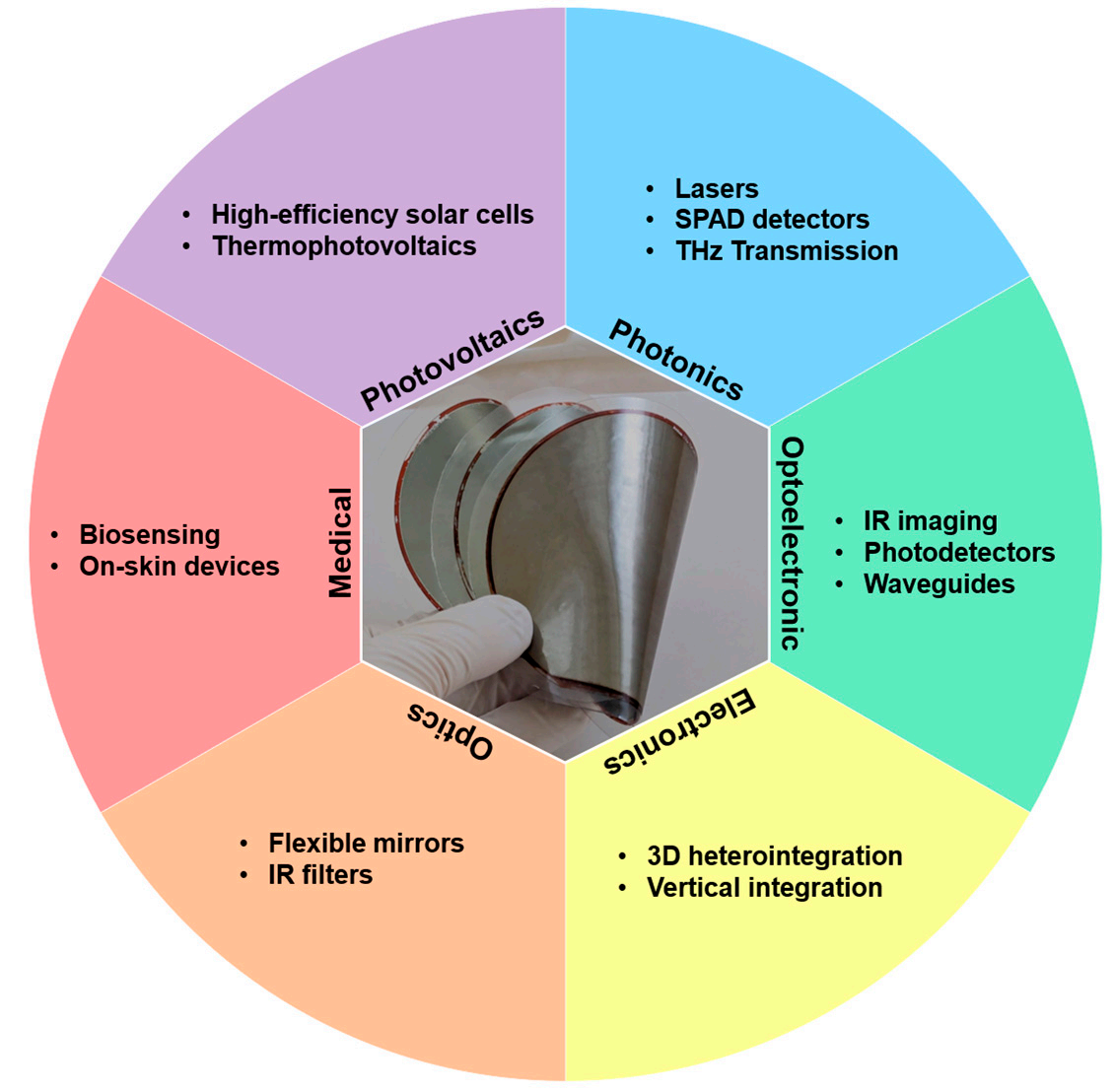
Figure 1. llustration of Ge FSM applications. The central image depicts freestanding Ge membranes on a fexible holder obtained in this work.
Various techniques have been demonstrated for Ge FSM fabrication, including substratethinning, epitaxial liftoff, Smart cut technology, mechanical spalling, 2Dassisted epitaxy, and Germanium-on-Nothing. Among them, the porosification lift-off technique has recently received significant attention and development thanks toits potentially high-throughput and cost-effective process. This approach involvesthe formation of a uniform and tunable porous Ge (PGe) layer using electrochemical etching, followed by the deposition of a Ge membrane on top of it. The membranecan then be detached from the parent substrate through the weak nanostructured interfaceforming a thin Ge FSM. Moreover, this technique enables the reconditioning of the parentsubstrate by chemical etching and its reuse for the production of multiple Ge FSM further reducing the fabrication cost by avoiding the need for costly chemical-mechanicapolishing. Overall porosification liftoff has shown its potential for large-scaleproduction of Ge FSM, with the significantly reduced consumption of Ge material thanstandard wafering techniques. Even with all the recent advancements this technique holdsthe potential to be imprved and further reduce the quantity of Ge during the pmductionof Ge FSM.
2. Materials and Methods
PGe layers were formed using an optimized bipolar electrochemical etching (BEE) process on top of Ge substrates. The p-type gallium (Ga) doped, 100 mm Ge wafers oriented along the (100) axis, with 6◦ off-axis miscut towards (111) orientation and resistivity of 8–30 mΩ·cm were used in this study. Before the PGe formation, the Ge substrate was deoxidized in a concentrated hydrofluoric acid (HF, wt%) solution for 5 min, followed by rinsing in anhydrous ethanol (EtOH, 99 wt%) and drying under nitrogen (N2) flow. The BEE was carried out in a custom-built 100 mm porosification cell, consisting of a polytetrafluoroethylene (PTFE) body, copper (Cu) backside electrode, and platinum (Pt) wire working electrode, filled with 300 mL of electrolyte solution composed of HF (49 wt%):EtOH (99 wt%) in 4:1 (V:V) proportions. The SP-50 BioLogic generator was used to apply cyclic square 1 s pluses of etching and passivation with 1.5 and 1.0 mA·cm−2 current density, respectively. Each cycle was separated by 1 s rest time and 420 cycles were applied in total to produce the PGe layer. At the end of the process, PGe substrates were rinsed with EtOH (99 wt%), dried under N2 flow, and subsequently placed into the loading chamber of the growth reactor under a vacuum. Further details on PGe formation can be found in our previous work.
After epitaxial growth, the Ge FSM is detached using an adhesive tape and is transferred onto a flexible Polyvinyl Chloride (PVC) substrate. The recovered Ge substrate has been reconditioned by immersion in a concentrated hydrogen peroxide (H2O2, 30 wt%) solution for 1 min, at room temperature, to transform the remaining PGe crystallites at the surface in germanium dioxide (GeO2) and etch them slowly away. The substrate has been subsequently deoxidized in concentrated HF (49 wt%) to dissolve the remaining Ge oxides on the surface and recover a flat surface. The reconditioned substrate is then reporosified, using the same BEE conditions as on the epi-ready substrate. The complete list of specifications of all the chemicals used in this study can be found in Table S1 of Supplementary Materials.
3. Results and Discussion
The fabrication process of Ge FSM through the porosification lift-off technique consistsof four main steps, as illustrated in Figure 2. First, a high-porosity (60-80%) porousgermanium (PGe) layer is formed at the Ge substrate surface by electrochemical etching ina HF:EtOH electrolytic solution. This is followed by a low-temperature deposition of theGe membrane on top of the PGe layer. The membrane is then mechanically detached fromthe substrate, which is facilitated by the fragile nanostructured PGe interface between theGe bulk substrate and the Ge FSM,. After detachment, the PGe remnants at the surface olthe recovered parent Ge substrate are oxidized using an H0, solution followed by theircomplete dissolution in HF and reuse of the parent Ge substrate for reporosification andrepeating the process of Ge FSM fabrication. All steps were previously detailed in theMaterials and Methods Section, and the obtained results are discussed further below.
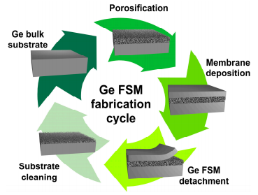
Figure 2. Schematic illustration of the Ge freestanding membrane fabrication and substrate reuse.
The Ge FSM fabrication cycle begins with the formation of a high-quality PGe layeron top of the Ge substrate. This is a crucial part of the process, as any major defectsor inhomogeneities in the PGe structure can be further transferred to the Ge membraneimpacting its quality. Figure 3a shows a SEM cross-sectional micrograph of the PGelayer used in this work. The typical sponge-like porous structure shows a well-definedinterface between the PGe layer and bulk material, with ~264 nm thickness and 63%porosity. Furthermore, the ellipsometry mapping of the 100 mm wafer, shown in Figure 3b cdemonstrates the overall uniformity of the porous nanostructure in both the thickness andporosity with respective variations of +4 nm and +1% across the entire surface of thewafer. oreover, the porous structure manifests a low surface roughness below 2 nm, asillustrated by Figure 3c. The closely packed crystallites of the high-porosity PGe layers(60-80%) make an excellent template for the growth of Ge membrane structures whileenabling an easy detachment without additional annealing steps or deposition of thestressor layers to initiate the separation.
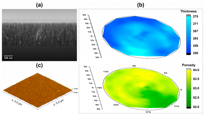
Figure 3. (a) Cross-sectional SEM micrgraph of the PGe structure (b) Ellipsometry mapping ofthe 100 mm wafer showing the uniformity of the PGe layer in thickness (blue) and porosity (green)(c)5 x 5 um? AFM scan of the PGe surface.
A 1 um thick Ge membrane is then grown, at 300 °C, on top of the PGe structureresulting in a smooth surface with RMS roughness around 0.7 nm, as demonstrated byFigure 4a. A few shallow pits and undulations are still identifiable on the surface but can beannihilated by increasing the membrane's thickness. Depending on the targeted applicationthe thickness of the membrane can be varied from .100 nm to few um. However, formembranes thinner than 1 um the surface roughness can increase up to 5 nm for thethinnest membranes. This way, the amount of Ge material used for device integrationcan be directly controlled to use only the quantity of Ge necessary for its function andhence,limit the waste ofmaterial.
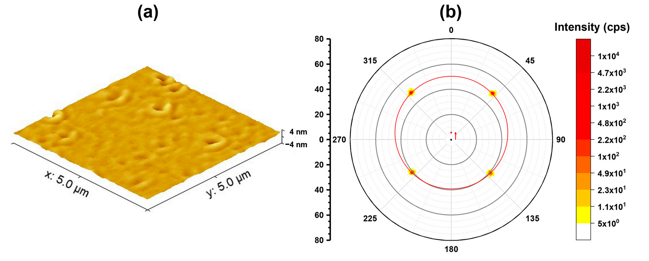
Figure 4. (a) 5 x 5 um’ AFM scan of the Ge membrane grown on PGe with surface roughness <l nm(b) In-plane pole figure of the Ge FSM around Ge (220) axis, the red circle and arrow represent the 6°offcut orientation of the membrane compared to normal axis.
The entire chemical cleaning process is schematically illustrated in Figure 6a. The AFMscan of the recovered substrate in Figure 6b shows a flat surface with surface roughnessbelow 1 nm. The apparent waving of the cleaned surface represents a slight variation inthe initial Ge bulk /PGe interface formed during the BEE process, as the bottoms of thepores are not all perfectly aligned. This effect is then partially mitigated directly by the firstanodic step of the BEE process during the formation of the new PGe layer.
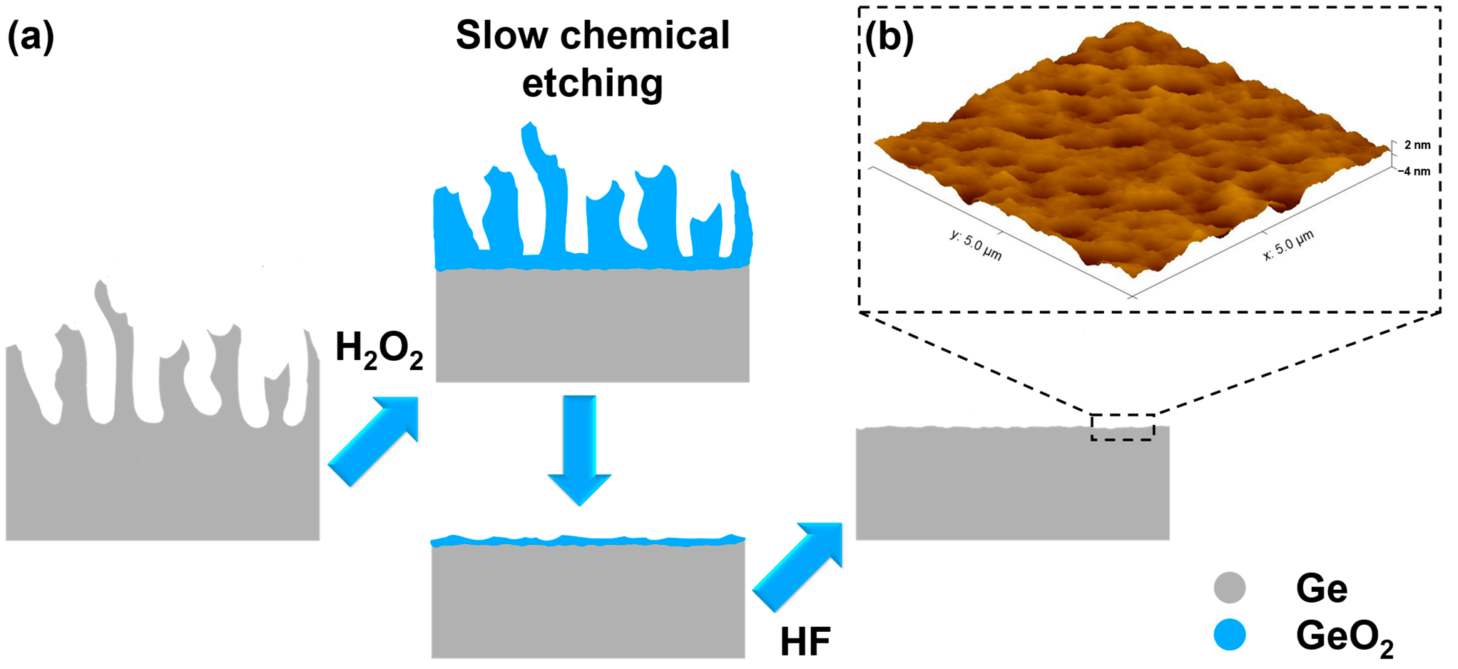
Figu re 6. (a) $chematic illustration of the slow chemical etching cleaning process ofthe PGe remnantson the substrate's surface (b)5 x 5 um’ AFM scan of the recovered Ge substrate after chemicalcleaning with RMS rughness of 0.8 nm.
In numbers, around 300 nm of the original substrate is consumed per producedmembrane. This value includes the thickness of the PGe layer (~270 nm) and the front/backetchingofthe substrate during the cleaning process (~30 nm). Byconsidering a conventional100 mm Ge wafer with a thickness of 175 um, and its thinnest commercially availablecounterpart with a thickness of 140 um, around 35 um of the substrate can be used for GeFSM production before losing its structural integrity. This results in over 100 membranes produced from a single 100 mm wafer. The number of reuses can be further increased bythe use of thicker substrates, which bring additional benefits such as a reduction in materiallost during the sawing process of Ge wafers from a solid ingot grown by the Czochralskimethod [56-58]. Alternatively, the Ge substrate can be bonded on a holder (e.g., Si substratefor mechanical support, allowing for the use of almost the entire substrate's thickness andenabling over 500 reuses. This number is expected to fur ther grow with scaling on largersubstrates,as larger diameter wafers are considerably thicker.
Conclusions
In conclusion, we demonstrated a successful substrate reuse and production of a highly uniform PGe layer on recovered Ge substrate, setting the milestone for the production of multiple Ge FSM from the same substrate. The reduced thickness of the PGe structure allows for a reduction in Ge consumption per cycle, compared to previous studies, while still maintaining the capacity to easily detach and transfer the membrane. Additionally, the optimized porosity helps to improve the surface quality of the Ge FSM membrane. The substrate cleaning is achieved through slow chemical etching of the PGe remaining on the surface, enabling its complete dissolution and obtention of the surface with roughness below 1 nm, without the necessity of substantial etching of the substrate material. The recovered substrate enables the successful reporosification of the entire 100 mm wafer, resulting in a new high-quality PGe layer with physical properties identical to the one formed on the epi-ready surface. This allows for efficient substrate reuse, and the production of multiple Ge membranes, with minimal consumption of the Ge material, due to the optimized PGe structure employed in this work. The Ge FSM production and substrate recovery opens the way for a sustainable alternative to conventional Ge substrates while providing all the advantages of freestanding form for direct heterointegration and flexible electronics. It offers to significantly lower the quantity of Ge material integrated into optoelectronic devices, reducing the quantity of hard-to-recover material in end-of-life products. Furthermore, this approach presents a high potential for the fabrication of FSM from other group IV materials, such as Ge(Si)Sn alloys, presenting a small bandgap ideal for near/mid-IR optoelectronic and photonic applications offering a non-toxic and low-cost alternative to III-V materials.
下一篇: 薄型晶硅太阳能器件的进展、挑战和前景