The increasing adoption of solar energy as a renewable power source marks a significant shift toward clean, sustainable alternatives to conventional energy forms. A notable development in this field is the advancement of thin monocrystalline silicon (c-Si) solar cells. Characterized by their lightweight, flexible nature, these solar cells promise to transform the renewable energy landscape with enhanced durability, adaptability, and portability. Amidst the growing demand for sustainable energy solutions, refining and evolving thin c-Si solar cell technologies is crucial. This review comprehensively examines the latest progress in thin c-Si solar energy conversion device technologies, offering an extensive overview of current methodologies for producing thin c-Si films, advanced light trapping techniques, surface passivation strategies, and methods for managing thin wafers. It also explores the wide-ranging applications of thin c-Si solar cells. Furthermore, this article sheds light on the techno-economic aspects, highlighting the intertwined challenges of commercializing these innovative cells. Through an in-depth analysis of the latest advancements, this review serves as a valuable resource for researchers and industry experts, keeping them abreast of current trends and catalyzing further advancements in thin c-Si solar cell technology.
1. Introduction
Addressing global warming and ensuring energy security are two of the most pressing challenges facing our world today. The reliance on carbon-rich fossil fuels has exacerbated these issues, making the transition to renewable and environmentally friendly energy sources an urgent priority. With its vast potential, solar energy stands out as a leading solution. The earth receives plentiful solar energy, ≈9600 times more annually than the global energy consumption of 17.91 TW in 2017.This immense energy resource offers a sustainable pathway to meet our energy needs while mitigating environmental impact.
At the forefront of harnessing this solar energy are photovoltaic devices, particularly those based on monocrystalline silicon (c-Si). Dominating the solar market, c-Si solar cells are valued for their low cost, widespread availability, mature industrial production processes, non-toxic nature, and stable performance over long periods, often exceeding two decades.Recent technological advancements have significantly boosted the efficiency of c-Si-based photovoltaic devices, achieving up to 26.8% efficiency.This progress inches these devices closer to the theoretical maximum efficiency of 29.4%, as defined by the Shockley–Queisser limit. Such improvements are primarily attributed to advancements in manufacturing technologies, especially in surface passivation and photon management, enhancing both the voltage and current output of these solar cells.
Despite their widespread use and covering over 90% of the global market, c-Si-based photovoltaic devices account for around only 4.5% of global electricity generation.While cSi photovoltaic modules are currently the most cost-effective method for producing electricity, there remains significant potential to further reduce the cost of electricity generation using these modules. This would not only increase their contribution to global electricity production but also enhance accessibility to solar energy worldwide. The thickness of the silicon wafers utilized in manufacturing the cells has a notable impact on the cost of these c-Si photovoltaic modules.Conventionally, these wafers are ≈165-μm thick, accounting for a significant portion of the total manufacturing cost..However, recent developments have shown that using thinner wafers, ≈50-μm or even as thin as 10-μm, could substantially reduce production costs without compromising the device’s performance.
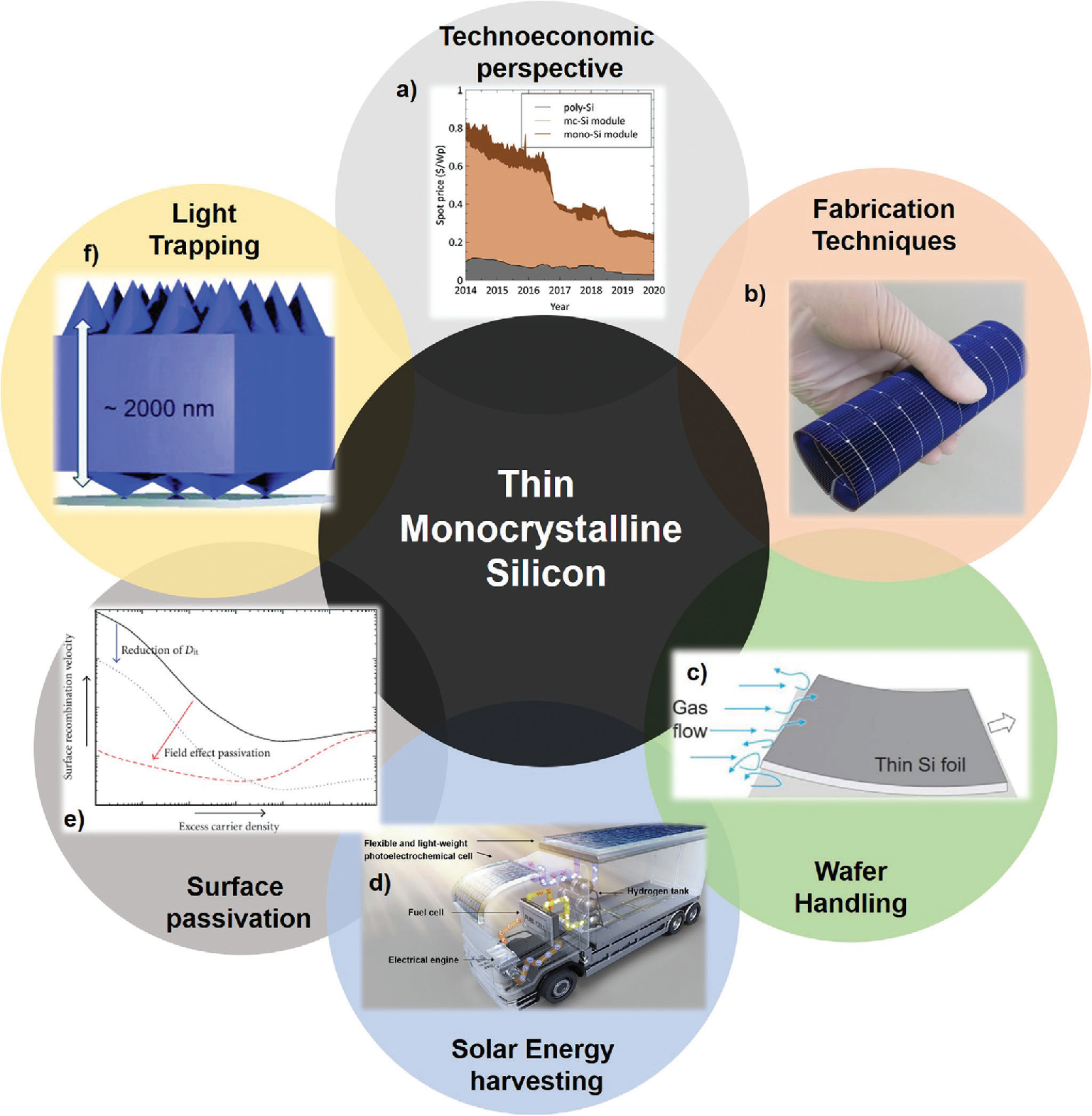
Given the rapid evolution of thin c-Si solar cell technology, it is essential to comprehensively review and understand the recent research and technological advancements in this field. This article aims to cover the latest developments in thin c-Si solar energy conversion devices. It covers a broad spectrum of topics, from innovative methods for producing thin c-Si films to advanced strategies for light absorption, state-of-the-art surface passivation techniques, and effective handling of thin wafers, as illustrated in Figure 1. Additionally, this review delves into the technoeconomic aspects of these technologies, examining their economic viability and scalability. It also highlights the challenges in commercializing thin c-Si photovoltaic technologies and offers insights into overcoming these obstacles to facilitate widespread adoption. By providing a comprehensive assessment and current perspective on thin c-Si solar cell technology, this review aims to inform and guide researchers, industry professionals, and stakeholders in their quest to harness solar energy more efficiently and sustainably.

Figure 1. Overview of different aspects of thin c-Si solar energy devices. a) Reproduced with permission from. Copyright 2022, Elsevier. b) Reproduced with permission from.Copyright 2023, Springer Nature. c) Reproduced with permission from.Copyright 2019, Elsevier.d) Reproduced with permission from.Copyright 2021, Elsevier. e) Reproduced with permission from.f) Reproduced with permission from.
In 2020, Liu and colleagues conducted an extensive technoeconomic analysis to reassess the proposition of using thin c-Si in the modern photovoltaic industry, quantifying its benefits.Their findings revealed that a thickness of 50-μm provided the optimal reduction in module cost, capital expenditure (CAPEX, inclusive of module and balance of system costs), and levelized cost of electricity (LCOE, considering both CAPEX and operational expenses) across various technologies (Figure 2 and Table 1). Take for instance a typical PERC cell, as prevalent in 2018, with an efficiency of 19%; reducing wafer thickness from 160–50-μm resulted in a module cost reduction of 0.07 $ W−1 (reaching 0.26 $ W−1) and a CAPEX reduction of 0.14 $/(W/year) (reducing to 0.26 $/(W/year)). The LCOE for the 50-μm thickness was 5% lower than the current LCOE for all technologies examined in the study (reaching 5.2 ¢/kWh for PERC). This achievement is particularly noteworthy, given that the photovoltaic industry shifted from Al-BSF to PERC architectures with a 3% gain in LCOE. Consequently, these calculations present a compelling economic case in favor of thin c-Si technology. It should be noted that the PERC technology’s market share has been rapidly decreasing since 2022 and is expected to be surpassed by the TOPCon technology ≈2027.The thickness of TOPCon silicon wafers is ≈120-μm, lower than PERC wafers but still presenting the potential for further thinning and associated cost reductions.

Figure 2. Manufacturing CAPEX, module cost, and U.S. utility LCOE for the three solar cell concepts with varying c-Si thickness. Reproduced with permission from.Copyright 2020, Royal Society of Chemistry.
The emergence of thin c-Si photovoltaics may, therefore, necessitate a re-evaluation and restructuring of existing photovoltaic waste recycling processes and technologies.These considerations are crucial given that module manufacturers bear the responsibility for recycling services.
3. Thin c-Si Fabrication Techniques
Conventionally, c-Si wafers are obtained from their ingot using wire sawing. While doing so, some materials are lost from the ingot as waste, known as kerf-loss. This waste could be as high as 40% while slicing 180–200-μm thick c-Si wafers and could be even more for thinner wafers.Owing to significant kerf-loss, the industrially adopted wire sawing method is not a preferred technology to obtain thinner wafers. To further reduce the cost of c-Si solar cells, alternative industrially compatible technologies to fabricate thin c-Si without kerf-losses need to be developed. This section discusses different technologies developed so far to fabricate thin c-Si and solar cell devices fabricated using these thin c-Si.
3.7. Chemical Etching
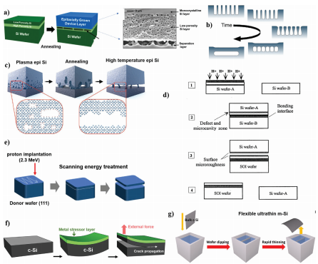
Chemical etching is an easy and facile method of thinning down the thick c-Si wafer. The processing steps are shown in Figure 3g. As shown in the Figure 3g, bulk wafers are directly immersed into alkaline solutions (mainly potassium hydroxide; KOH) at an elevated temperature (80–90 °C) for several hours to achieve the desired thickness. The typical etching rate of a c-Si wafer is ≈1 to 2-μm per minute. This process has been extensively used to obtain thin c-Si wafers as a platform for the proof of concept of emerging solar cell technologies on thin c-Si. In 1996, Wang et al. adopted this technique to obtain a 47-μm thick free-standing c-Si solar cell with a record PCE of 21.5% (Table 2).The authors adopted the passivated emitter, rear locally diffused (PERL) technology to fabricate the solar cell, which was one of the widely used technologies to fabricate highly efficient Si solar cells. In 2019, Jian et al. utilized chemically etched 25-μm thick c-Si to fabricate a dopant-free asymmetric heterojunction-based solar cell with a PCE of 15% (Table 2).In the study, the authors demonstrated the applicability of poly(3,4-ethylenedioxythiophene):poly(styrenesulfonate) (PEDOT:PSS) and fluorine-doped titanium oxide as holeselective and electron-selective passivating contacts, respectively. Recently in 2021, Sai et al. employed this technique to fabricate a 50-μm thick c-Si solar cell with a PCE of ≈23.3% and an unprecedented open circuit voltage (Voc) of 754 mV (Table 2).While chemical etching is suitable for obtaining defect-free thin c-Si for demonstrating different emerging solar cell technologies, it is not suitable for industrial purposes owing to the severe material loss in the process.

Figure 3
Rinke et al. first introduced this process in 1999 at the University of Stuttgart, Germany.This process is similar to the SPS process except for one difference: in this process, the sintered porous Si layer does not act as a seed layer for epitaxial growth but rather the layer itself is split off from the wafer as shown in Figure 3b. This process is advantageous over the SPS process as no epitaxial growth is required. In one study, Hemment et al., demonstrated that 30 sintered porous thin c-Si could be obtained from a single c-Si wafer.They also reported a short circuit current density (Jsc) of 11.1 mA cm−2 could be obtained from 4-μm thick p-type c-Si films. Similarly, researchers at IMEC, Belgium, demonstrated a 20-μm thick solar cell with a PCE of ≈12.6% (Table 2).Later, the same group demonstrated a flexible and semitransparent 830 nm-thick c-Si with a PCE of 8.6% (Table 2). One drawback of this process is that the lifted-off layer possesses defects in the form of small pores which would lead to lower performance. Moreover, after the removal of the thin c-Si layer, the surface of the host Si wafer is rough and would require mechanochemical polishing to make the surface smooth for the next batch of processing, which adds to the cost of processing and significant material loss.
Chemical Etching
Chemical etching is an easy and facile method of thinning down the thick c-Si wafer. The processing steps are shown in Figure 3g. As shown in the Figure 3g, bulk wafers are directly immersed into alkaline solutions (mainly potassium hydroxide; KOH) at an elevated temperature (80–90 °C) for several hours to achieve the desired thickness. The typical etching rate of a c-Si wafer is ≈1 to 2-μm per minute. This process has been extensively used to obtain thin c-Si wafers as a platform for the proof of concept of emerging solar cell technologies on thin c-Si. In 1996, Wang et al. adopted this technique to obtain a 47-μm thick free-standing c-Si solar cell with a record PCE of 21.5% (Table 2).The authors adopted the passivated emitter, rear locally diffused (PERL) technology to fabricate the solar cell, which was one of the widely used technologies to fabricate highly efficient Si solar cells. In 2019, Jian et al. utilized chemically etched 25-μm thick c-Si to fabricate a dopant-free asymmetric heterojunction-based solar cell with a PCE of 15% (Table 2).[50] In the study, the authors demonstrated the applicability of poly(3,4-ethylenedioxythiophene):poly(styrenesulfonate) (PEDOT:PSS) and fluorine-doped titanium oxide as holeselective and electron-selective passivating contacts, respectively. Recently in 2021, Sai et al. employed this technique to fabricate a 50-μm thick c-Si solar cell with a PCE of ≈23.3% and an unprecedented open circuit voltage (Voc) of 754 mV (Table 2).While chemical etching is suitable for obtaining defect-free thin c-Si for demonstrating different emerging solar cell technologies, it is not suitable for industrial purposes owing to the severe material loss in the process.
Handling Thin Wafers
The introduction of thin c-Si wafers is aimed to enhance the flexibility of brittle c-Si solar cells, facilitating their integration onto flexible surfaces. However, handling and processing thin (<100- μm) c-Si substrates present significant challenges due to their increased vulnerability to external mechanical shocks compared to c-Si substrates with conventional thickness (180–500-μm). These thinned c-Si wafers are highly susceptible to external mechanical loads during fabrication and handling processes, posing diffi- culties in adapting them to current manufacturing processes. To overcome these challenges, the development of appropriate handling methods is crucial to ensure the successful transformation of thin c-Si substrates into flexible solar cells with high throughput and satisfying processing yield. This section discusses current trends in thin c-Si substrate handling for flexible solar cells and examines the associated challenges.
Thin c-Si Wafer Handling as Free-Standing Film
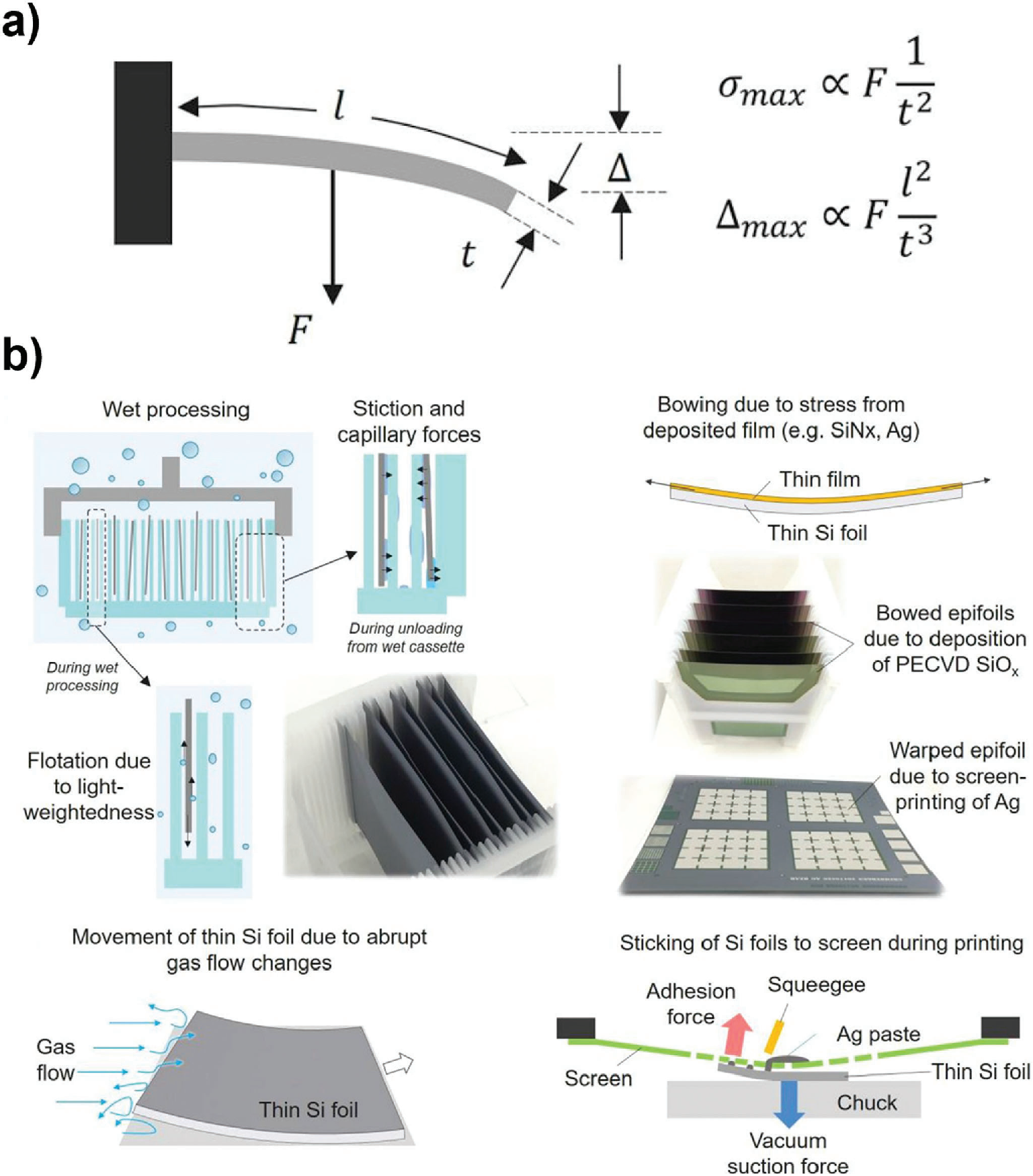
The enhanced flexibility of c-Si substrates, achieved through significantly reduced thickness, introduces notable challenges in thin substrate processing and transportation. Figure 7a illustrates the conventional bending test of the substrate, highlighting that the maximum deflection (Δmax) of the substrate is proportional to the cube of the substrate thickness (t3).For thin c-Si substrates, their weight can induce undesirable wafer bending due to reduced substrate thickness and the influence of gravity. Handling these thin c-Si substrates becomes increasingly challenging during high-speed transport, as stresses from air resistance and vibrations can cause significant bending, further complicating the handling of these flexible substrates. The impact of these stresses can limit a handler’s maximum speed and acceleration and, as a result, reduce the overall throughput. Furthermore, significant gravity sag may render thin substrates’ loading and unloading processes from conventional cassettes impractical.

Figure 7. a) Schematic illustration of mechanical behavior of a single beam showing the dependency between the load, F, length, l, and thickness, t, maximum stress, 𝜎max, and maximum defection, Δmax. b) Schematic illustration showing the challenges encountered during thin wafer handling and processing, including floating during wet processing, bowing after thin-film deposition, movement due to abrupt gas flow changes, and adherence to screen during metal-paste printing. Reproduced with permission from.[18] Copyright 2019, Elsevier.
Generally, individual solar cells are connected in series and parallel as modules to derive the desired output power for outdoor applications. Conventionally, solar cell module packaging technologies are based on the thick glass at the front and metal frame at the rear and edges, which are rigid and heavy. Therefore, the conventional way would not be appropriate for flexible solar cell modules. Additionally, these flexible thin c-Si solar cells are very delicate and would require extra precautions during handling and processing. The module packaging technology utilizing flexible and lightweight polymeric carriers such as PDMS or polyethylene terephthalate would not only benefit packaging the flexible solar cell modules but would also be advantageous in integration on textiles, vehicles etc.