Abstract.
In this work, the growth of a magnetron sputtered NiAl film on Ge was investigated. Two growth parameters were varied: the deposition temperature and the presence of native GeOx. An epitaxial layer was obtained at a deposition temperature of 400◦C and without removal of the native GeOx prior to deposition. At this growth condition, Ni and Al diffused into the Ge forming an epitaxial germanide. This germanide is most likely the τ3 phase of the Ni-Al-Ge ternary system. The growth of the τ3 phase is enabled by the GeOx acting as a diffusion barrier for Al. The native GeOx was found to be amorphous and to contain holes through which the NiAl can directly contact the τ3 germanide and grow epitaxially. These holes are likely formed by thermal degradation when the substrate is heated for deposition. The electrical resistivity for epitaxial NiAl was found to be 13 µΩ.cm at a thickness of 30 nm which was the lowest value of the tested conditions. Epitaxial NiAl can be used as a seed layer to grow other layers epitaxially in a CMOS-compatible process, e.g. Fe(Co), Cr, MgO, and Heusler alloys.
1. Introduction
Epitaxial growth of thin films is the pinnacle of material deposition. Typically, this is achieved, for metallic thin films, using molecular beam epitaxy (MBE) on a substrate with sufficiently small lattice mismatch with respect to the desired material. These conditions are not suitable for CMOS-compatible applications due to the low deposition rate of MBE and the difficulty of scaling to 300 mm Si wafers. Especially the use of Si wafers cannot be deviated from for microchip fabrication in part due to its low cost and mechanical stability. Due to these constraints, epitaxial growth processes have been limited to the laboratory scale.
In this work, the deposition of NiAl on Ge(001) was investigated with the goal of growing epitaxial NiAl. This was done by depositing 30 nm of NiAl at various growth conditions. Deposition temperatures of 200℃ and 400℃ were examined as well as the effect of the presence of native Ge oxide (GeOx) on the growth. The surface morphology was characterized by atomic force microscopy (AFM) and layer thickness was determined by X-ray reflectivity (XRR). X-ray diffraction (XRD) and transmission electron microscopy (TEM) were used to examine the crystallinity of the NiAl. Energy-dispersive X-ray (EDX) spectroscopy provided information on chemical composition. Lastly, the electrical sheet resistance was measured as an additional indication of NiAl crystallinity.
2. Experimental
Then, the Ge layer thickness is reduced to 700 nm using chemical-mechanical polishing (CMP) to obtain a smooth surface with a threading dislocation density of 107 cm−2. The native GeOx is formed from exposure to air. Next, NiAl deposition was done in a EC7800 (Canon Anelva) DC magnetron sputtering tool at a base pressure of 10−7 Pa. The working pressure was in the order of 0.1 Pa with Ar as the sputter gas. At this working pressure, the mean free path of Ar is a few centimeters while the targetto-wafer distance is around 20 cm. This large distance compared to the mean free path reduces unwanted backscattered Ar from reaching the substrate. A single NiAl target was used with a 1:1 atomic composition. In cases where the native GeOx needed to be removed, the wafers were in-situ annealed for 20 min at 600℃, in ultra-high vacuum, followed by a 10 min cool-down. This temperature was chosen in order to guarantee full desorption of the native oxide. 30 nm of NiAl was deposited with a substrate temperature of either 200℃ or 400℃. For each substrate temperature, there were two wafers, one with and one without native oxide removal. The hypothesis was that NiAl growth on Ge is analogous to growth on Si i.e., epitaxial growth when deposition is done at 400◦C on an oxide-free substrate. Figure 1 gives an overview of the tested growth conditions.
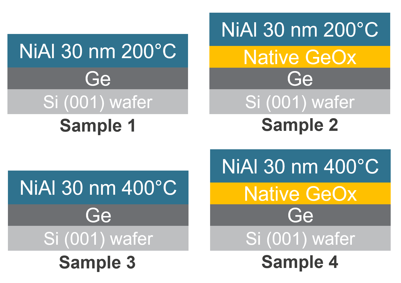
Figure 1. Overview of the four growth processes. The native GeOx is removed from sample 1 and 3 prior to NiAl deposition. Sample 1 and 2 have NiAl deposited at 200◦C while on sample 3 and 4 deposition is done at 400℃.
3. Results
Figure 2 shows AFM images of the 4 samples. Sample 1 and 2 had a similar arithmetic average (Ra) and root mean square (Rq) surface roughness. This is shown in figure 2a) and b) with Ra values of 0.410 nm and 0.502 nm respectively. Sample 3 and 4, figure 2c) and d), had comparatively higher roughness with Ra values of 4.13 nm and 1.23 nm, respectively. The roughness of sample 3 had two origins. Firstly, the NiAl grains did not fully merge resulting in voids, as shown by the line profile in figure 2 e). Second, the individual grains themselves did not have a uniform height with variation up to 10 nm as seen in figure 2 e). The line profile of sample 4 shows that grain height was more uniform than sample 3, figure 2 f). Voids are still present in sample 4 reaching depths of 10 nm which was similar to sample 3.
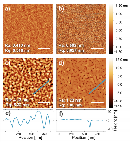
Figure 2. AFM images of samples 1,2,3, and 4, a),b),c), and d), respectively. The white scale bar represents 500 nm. a) and b) use the upper height scale, c) and d) use the lower height scale. e),f) Line profiles obtained at the blue line of c) and d) respectively.
This is evidenced by the Fast Fourier Transform (FFT) images in the inset of figure 6a). FFT is done at two locations in the NiAl layer showing that the crystal orientation is not uniform. Figure 6b), TEM image of sample 2, shows a presence of the native GeOx at the Ge/NiAl interface with a thickness of 1 nm. The NiAl is not epitaxial nor does it show any preferential crystal orientation, as confirmed by the circular features of the FFT image. Limited germanidation below the GeOx is observed. Figures 6c)-d) show NiAl deposited at 400℃with and without oxide degas i.e., sample 3 and 4 respectively. For sample 3, figure 6c), the NiAl grains had a lateral size of around 20 nm and have various crystal orientations. Moreover, the Ge/NiAl interface was very rough with some voids (not shown), which indicates an intense chemical reaction between the Ge template and the deposited metals. In figure 6d), the NiAl layer was found to be in an epitaxial relation with the Ge substrate. In the FFT image NiAl (001) and (220) were identified confirming the same epitaxial relation as found with XRD. The GeOx layer, 1 nm thick, was interrupted at several locations by the NiAl.
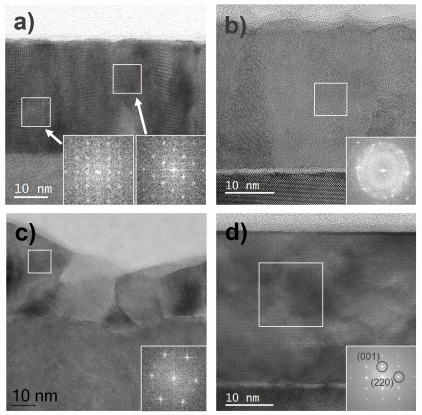
Figure 6. Bright field TEM images of sample 1,2,3, and 4, a),b),c), and d), respectively. The white squares indicate where the FFT image, shown in the inset, is taken.
This concentration peak coincides with the O peak at the NiAl top surface from natural oxidation after deposition. A second O layer was present between the Ge and the NiAl originating from the native GeOx, figure 7a)-b). At the native GeOx, Ge and Al were present while Ni saw a sharp dip in concentration, figure 7b). According to the 2D map, figure 7b), Ni did diffuse non-uniformly in the Ge layer as did Al, to a lesser extent.
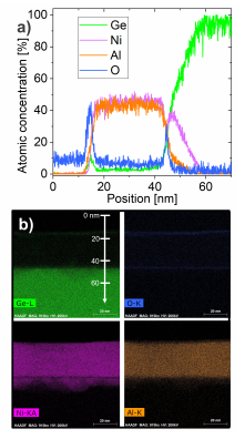
Figure 7. EDX maps of sample 4 showing germanidation below the NiAl layer. a) Is a line scan and b) shows 2D maps of each element. The white vertical scale indicates the scan direction of a).
4. Discussion
In sample 2, GeOx was not degassed prior to deposition at 200◦C, epitaxial growth was not observed as evidenced by XRD and TEM, figure 3 and 6b). This is unsurprising as the amorphous GeOx prevents the NiAl to contact the Ge for epitaxial growth. The other three samples (1,3, and 4) did show an epitaxial relation between Ge and NiAl as shown in figure 5.
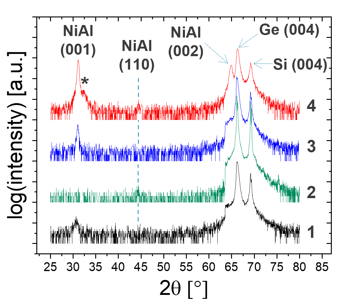
Figure 3. XRD 2θ-θ-scan of samples 1,2,3, and 4. A sample tilt of ψ = 1◦ was used in order to reduce the Si(004) and the Ge(004) peak intensity.
The rocking curve of sample 1, figure 4, had the widest NiAl (001) peak (FWHM=2.23◦ ) compared to sample 3 and 4 indicating that sample 1 is less crystalline with increased mosaicity. This is due to the low deposition temperature of sample 1 (200℃) compared to sample 3 and 4 (400℃). Epitaxial growth was shown according to the XRD scans, figure 5a) and c). However, the TEM revealed that the NiAl grains in sample 1 had varying crystal orientations, figure 6a). Therefore it can be concluded that a fraction of the grains did grow epitaxially, explaining the TEM and the XRD results.
5. Conclusion
In this paper, the growth of sputtered epitaxial NiAl on Ge is presented. Two growth parameters were varied: the deposition temperature and the presence of native GeOx. Only when the native oxide was not degassed, combined with 400◦C as the deposition temperature, did the film crystallize in a uniform crystal direction. The epitaxial relation was determined to be NiAl (001)//Ge (001) and NiAl (011)//Ge (011). With the other growth conditions no or only partial crystal alignment was found. Detailed TEM imaging revealed that an epitaxial germanide formed below the GeOx. NiAl was able to make contact with the germanide through local voids in the GeOx allowing the NiAl to grow epitaxially. The oxide voids were likely formed via thermal degradation before NiAl sputtering. A resistivity of 13.3 µΩ.cm at 30 nm nominal thickness is measured for the epitaxial NiAl which makes it a promising material for use as interconnects. NiAl can also be used as a seed layer to epitaxially grow various BCC metals and oxides e.g., MgO.