ABSTRACT
SiC is an indirect bandgap semiconductor with material properties ideal for power electronics but not so much as an optical emitter. Meanwhile, gallium arsenide (GaAs) is a material known for high-performance optical devices due to its direct bandgap and carrier lifetime. Integrating GaAs with silicon carbide (SiC) can result in the best of both materials. However, integrating the two presents a significant challenge due to the large lattice mismatch between the two materials. In this paper, we investigate the growth of high-quality GaAs directly on 4H-SiC and on AlAs/4H-SiC substrates. The thin films were characterized using key techniques for structural and optical analyses, such as x-ray diffraction, atomic force microscopy, and photoluminescence (PL) spectroscopy. The 3D-island nature of growth of GaAs directly on SiC results in weak in-plane correlation with the substrate but high photoluminescence. This was demonstrated with an observed PL intensity comparable to the PL observed from a GaAs substrate with a similar buffer layer. Introduction of a thin AlAs nucleation layer results in improved wetting of the substrate, better in-plane correlation with substrate, and overall improved crystalline quality and is now under further study.
I. INTRODUCTION
Silicon carbide (SiC) plays an important role in high-power and high-temperature applications in electronics, optoelectronics, and sensor devices. Interestingly, high-power devices can rely on optical communication for their wireless or waveguide connections, for example, between high voltage circuits and between sensor and monitor. Although SiC has significant capability for high power and high temperature, not so much as an optical emitter. This limitation can be overcome by GaAs, AlAs, AlGaAs, and InGaAs, which are well known for high-performance optical devices. The GaAs/SiC material system possesses important optical material properties, such as a large contrast in refractive index between GaAs and 4H-SiC, good thermal conductivity of the 4H-SiC substrate, and the transparency of the 4H-SiC substrate near UV to IR range, and importantly, SiC is highly resistant to radiation, temperature, and harsh environment, which can pair well with AlGaAs optical devices. The potential application we are seeking is for ultrafast sensors that can detect small temperature and strain changes quickly. Optical emitters, wave guides, and detectors on SiC can result in highly sensitive sensors that provide ultrafast corrective feedback.
However, a large mismatch in lattice constant and structure for GaAs/SiC presents a huge challenge to capitalize on these opportunities. Regardless of exciting applications, this bottleneck can potentially hinder investigative research for the growth of these dissimilar materials. However, given that the 4H-SiC substrate is expanding its potential applications in power electronics and highfrequency microelectronic devices, it is reasonable to revisit the possibility of growth of III–V semiconductor materials on SiC.
Growth of GaAs on 4H-SiC is anticipated along the [111] direction because of its similarity with the 4H-SiC sixfold lattice structure. In addition, growing GaAs (111) on 4H-SiC poses a substantial hindrance toward high-quality epitaxial growth because of the significant lattice mismatch potentially leading to strain relaxation, misfit dislocations, and threading dislocations. Moreover, an added challenge is due to surface and interface energy issues between GaAs on SiC and the potential for 3D growth. For instance, the surfaces of two materials can weakly or strongly interact with each other depending on surface and interfacial energy. Consequently, growth can nucleate locally resulting in overall 3D growth for GaAs on 4H-SiC. In addition, even for 2D growth, two azimuthal configurations rotated by 60° to each other or twins are likely to be introduced during the alignment of GaAs [111] direction to the 4H-SiC [0001] direction. Therefore, our effort is to optimize the growth conditions to overcome these challenges.
II. EXPERIMENT
All samples were grown by solid source molecular beam epitaxy (MBE). The 4H-SiC substrates were introduced into the load lock chamber and subsequently heated at 200 °C for 1 h to evaporate water vapor from the substrate surface. Subsequently, the cleaned substrates were transferred to the degassing chamber and were annealed at 1000 °C for 1 h to remove any organic contaminants and then transferred to the MBE growth chamber maintaining the vacuum. The substrates were then heated to the growth temperature according to the thermocouple reading. However, the actual surface temperature of the substrates may be about 50 °C less than the thermocouple temperature since the thermocouple is not in contact with the surface of the substrate. The growth rates of GaAs and AlAs were 0.8 and 0.2 ML/s, respectively. These growth rates were calibrated on the GaAs (100) substrates. The V/III beam equivalent pressure (BEP) ratio during GaAs growth was 20. The growth parameters are detailed in Table I, which includes growth temperature and layer thicknesses.
The surface morphology of each sample was investigated by atomic force microscopy (AFM) (Bruker, model number 3000 dimension III) using the tapping mode. AFM was performed using stable, sharp tips (Si tip material, tip radius ∼ 10 nm) with optimized feedback and force parameters. To measure the optical properties, the samples were mounted in a cryostat (Janis ST-500HT) for photoluminescence (PL) measurements at temperatures from 77 to 300 K using a confocal microscope (Horiba HR800). A 632.8 nm He–Ne laser was used as excitation, and the PL signal was collected by an electrically cooled Si CCD camera. To understand the structural properties and crystalline quality of grown materials, a PANalytical X’Pert MRD diffractometer equipped with a multilayer focusing mirror, a standard four-bounce Ge (220) monochromator providing a collimated and monochromatic incident Cu-Kα1 source of radiation (λ = 0.154 06 nm), and a Pixel detector was used for the x-ray diffraction (XRD) scans. The Raman data was acquired at room temperature using a spectrometer and an electrically cooled Si detector (Horiba Jobin-Yvon). The 2-μm-wide spot of the 632.8 nm probing laser was positioned on the desired area of the samples using a microscope system (Olympus 100×). Cross-sectional transmission electron microscopy was performed using a Titan80-3000 with an operating voltage of 200 kV to investigate the interface and the crystallinity of the grown structure.
III. RESULTS AND DISCUSSION
A. Direct Growth of GaAs on 4H-SiC
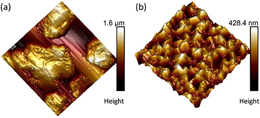
GaAs was first grown directly on thermally cleaned 4H-SiC. Two samples with nominal GaAs thickness of 400 nm, as calibrated from GaAs homoepitaxy, were grown at 600 °C (S1) and 650 °C (S2). The AFM images of surface morphology of the two samples are compared in Fig. 1. It is observed that the GaAs growth followed the Volmer–Weber mode (3D growth) indicated by the 3D islands. The formation of 3D islands is attributed to the large lattice mismatch and high interfacial energy. Well-defined faceted GaAs was evident only for sample S2 grown at the higher growth temperature. These facets of GaAs illustrate the crystalline nature of the islands. The root mean square (rms) roughness of samples S1 and S2 are 219 and 47.2 nm, respectively.

FIG. 1. AFM images (5 × 5 μm2 ) of samples grown at (a) 600 °C (S1) and (b) 650 °C (S2)
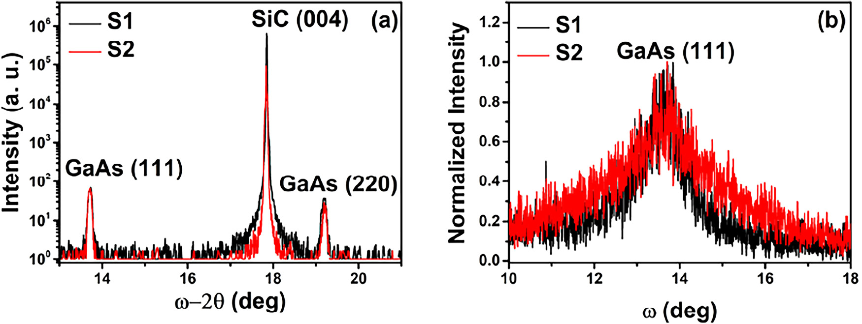
The crystallographic orientation of GaAs on 4H-SiC was studied by x-ray diffraction measurements. In particular, the XRD surface symmetrical ω–2θ scans of samples S1 and S2 are shown in Fig. 2(a). For both samples, the XRD spectra reveal the SiC (004) peak along with equally strong peaks of GaAs (111) and GaAs (220), which indicates that GaAs is growing along the [111] and [220] directions. This two-faceted growth is assigned to the weak interface between GaAs and SiC. From Fig. 2(b), broad rocking curves are observed signifying the material quality.

FIG. 2. X-ray diffraction (a) ω–2θ scan of samples S1 and S2 illustrating the presence of GaAs (111) and GaAs (220) along with the substrate peak and (b) ω scan showing the quality of the grown crystal.
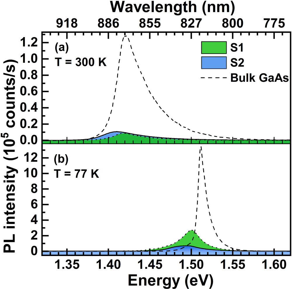
To examine the optical quality of the GaAs, the PL spectrum of the GaAs emission of each sample is shown in Fig. 3 in comparison to bulk GaAs. For both samples, the notably larger linewidth of the PL emission for the GaAs thin film compared to bulk GaAs indicates the effect of the misfit dislocations on creating alternative recombination channels within the bandgap, which reduces the carrier lifetime and is especially noticeable in Fig. 3 by the spreading of the low-energy tail at lower temperatures. At lower temperature (77 K), the PL intensity of S1 (2.72 × 10⁵ counts/s) is less than that of the bulk GaAs (13.68 × 10⁵ counts/s). As a result, at low temperature, we find that sample S1 has a PL that is only reduced by a factor of 5 from the PL from a reference sample of GaAs grown on GaAs.

FIG. 3. Temperature-dependent photoluminescence spectra of samples S1 (dotted filled curve), S2 (continuous filled curve), and bulk GaAs (dashed curve) at (a) 300 and (b) 77 K.
B. Growth of GaAs on 4H-SiC with a thin AlAs nucleation layer
Although we observe high photoluminescence for GaAs grown directly on SiC, it resulted in a poor XRD rocking curve. This is likely due to the different orientations of the GaAs 3D structures grown on SiC, each of which can be of good quality and, therefore, good PL but result in a poor rocking curve due to orientation as opposed to defects.
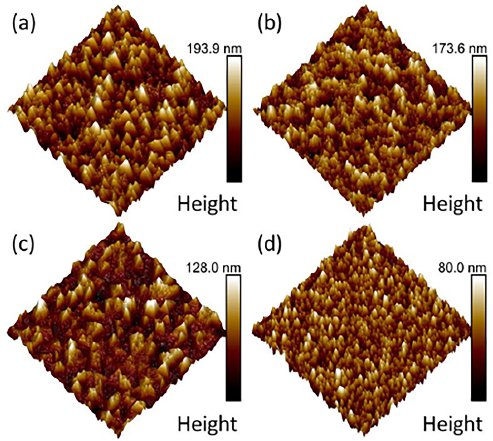
Because of the higher reactivity of aluminum than gallium or indium, we have added a thin layer of AlAs to provide improved wetting of the surface and reduce the formation of 3D island growth that is observed using GaAs directly on SiC. Four samples (S3, S4, S5, and S6) were grown with a thin AlAs nucleation layer between the 4H-SiC substrate and GaAs with the intent to reduce the interface energy. Figure 4 shows the AFM images of samples S3, S4, S5, and S6, which varied in thickness of the GaAs thin film from 400 to 100 nm. The rms roughness values of samples S3, S4, S5, and S6 are 22.5, 19.9, 15, and 11.5 nm, respectively. With the increase in thickness, strain energy increase that modifies the morphology and 3D islands becomes larger. When a thin layer of GaAs is grown, the island size is small. But as we increase the thickness of GaAs, coalescence and Ostwald ripening of islands take place due to higher growth time, and as a result, the height of the islands increases, which makes the roughness high.

FIG. 4. AFM images (5 × 5 μm2 ) of samples with GaAs growth temperature of 600 °C with different AlAs layer (a) S3, (b) S4, (c) S5, and (d) S6.
IV. SUMMARY AND CONCLUSIONS
This study is focused to achieve the growth of quality GaAs on SiC by MBE with potential for the development of optical sensors on SiC. Our observation is that GaAs growth on SiC resulted in a 3D growth as the lowest energy growth mode of GaAs. The underlying physics for this behavior is the large lattice mismatch between GaAs and SiC, which forces the lowest system energy to be a relaxed 3D structure. Therefore, despite the large lattice mismatch, the relaxed 3D structure can and does exhibit intense photoluminescence, only five times lower than PL observed from GaAs on a GaAs wafer. This indicates high-quality 3D growth, although the crystal orientation about the c-axis is not well defined, resulting in a rough surface profile. A smoother GaAs surface would also be desirable for the fabrication of optical source, waveguide, and detector. The application of a thin AlAs wetting layer to SiC, before the growth of GaAs, resulted in a much smoother surface and well-defined orientation about the c-axis. The AlAs improved the initial wetting of the surface due to the higher reactivity of aluminum than gallium. Based on this observation, we are now pursuing the underlying physics of the growth of an InAs/AlGaAs quantum well and quantum dots on the surface as well as the growth of InAs quantum dots directly on SiC, to take advantage of the preferred 3D growth, buried by a GaAs cap layer.