Abstract:
Micro-LED is considered an emerging display technology with significant potential for high resolution, brightness, and energy efficiency in display applications. However, its decreasing pixel size and complex manufacturing process create challenges for its integration with driving units. Recently, researchers have proposed various methods to achieve highly integrated micro-structures with driving unit. Researchers take advantage of the high performance of the transistors to achieve low power consumption, high current gain, and fast response frequency. This paper gives a review of recent studies on the new integration methods of micro-LEDs with different types of transistors, including the integration with BJT, HEMT, TFT, and MOSFET.
Introduction
Half a century ago, plasma display (PDP) technology was a popular display technology for time. PDP creates an image by exciting a phosphor to emit light through the discharge of ionized gases. Due to its high energy consumption and high costs, PDP was gradually replaced by other display technologies. Subsequently, liquid crystal display (LCD) monitors, which can regulate the brightness and color of pixels by controlling the arrangement of liquid crystal molecules and the polarization of light to display the image, became popular as the dominant display technology for nearly half a century. Now, organic light-emitting diode (OLED) display technology is an important display technology, which uses the electroluminescence of organic materials to produce images . It does not require a backlight and therefore has a higher contrast ratio, a wider viewing angle, and a faster response time. OLED consists of a stack of organics (ITO) sandwiched between a cathode and anode, where electrons and holes are injected from the electrodes into the organic layer for compounding and light emission. In recent years, the development of OLEDs has centered around two main areas: increasing the optical output power and thinning the device architecture. Currently, researchers are mainly using ordered structures such as (surface mounted) metal–organic framework (SUR) MOFs to regulate electron–hole mobility. This approach can enhance the optical output power while simplifying the structure of OLED devices. They also have great potentials for applications in the field of wearable devices and flexible displays.
In recent years, newly developed micro-LED displays have attracted a lot of attention. A micro-LED is a specially designed LED with an extremely small pixel size, which is capable of achieving high-definition, high-brightness, and high-contrast display perfor-mance. The high efficiency ofGaN-based-LEDs could offer low power consumptioncompared to other techniques. Currently, micro-LED displays have demonstrated greatpotential in near-to-eye applications, but they are still facing many challenges in terms ofmanufacturing and integration. Wearable devices, for example, virtual reality (VR) andaugmented reality (AR) devices, high-definition large displays, and other areas, requireextremely high performance from both micro-LEDs and driving units as well. With thecontinuous development and maturity of the micro-LED technique, it is expected thatmicro-LED displays will find a place in the future market and become the next dominantdisplay technology.
Micro-LED technology was firstly proposed by Prf. jiang and Prof. Lin in Texas TechUniversity. Generally, it is widely accepted that micro-LEDs do not exceed 50 microns in sizeFor different display applications, there are two main trends. One of the directions is thatwhich Sony is focusing on, which is small-pitch, high-resolution, large-size indoor/outdoordisplays. The other is the wearable devices (such as AR/VR and Watch) launched by Applewhich require high resolution, portability, low power consumption, and high brightness. Itis important to make the use of the many advantages of micro-LEDs: fast response time,high brightness, wide viewing angle, high dynamic range, low power consumption, andlong lifetime. The history of display technology is shown in Figure 1.
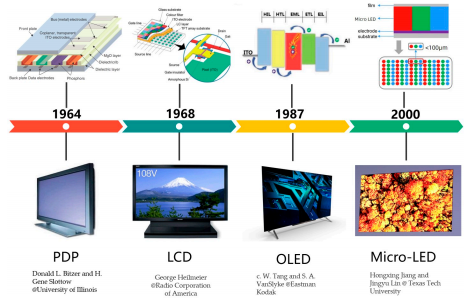
Figure 1. Development of display techniques.
Micro-LEDs are gradually replacing LCDs and OLEDs as the requirements for display resolution, brightness, and stability increase, but the EQE of quantum-well LEDs decreases as the size of the device is drastically reduced to around 100 µm. Quantum well LEDs will introduce a large number of dislocations and defects due to the ICP etching table, which will induce non-radiative surface bonding. There will be a certain lattice mismatch between InGaN and GaN in the quantum well, which means that InGaN quantum well LEDs face certain difficulties in efficiently emitting red and green light. To overcome this difficulty, nanowires/nanorods can be deposited on the substrate. Through selective growth, the size and morphology of the nanowires/nanorods can be precisely controlled to achieve the effect of changing the emission wavelength. By using SAG to produce highly uniform nanowires of the same polarity, the inhomogeneity associated with spontaneous nanowires can be eliminated. Such dislocation-free nanostructures can further enhance the performance and functionality of micro-LEDs, including narrow spectral linewidths and highly directional and stable emission.
Three-color stacking: The three-color stacking technology achieves the full color display by controlling each vertically stacked red, green, and blue micro-LED, as shown in Figure 2a. The stacking structure allows individual pixels to occupy less space, thereby achieving a higher pixel density per unit area, meeting the requirements for application in small-size micro-display devices and also having wide applications in the display field. Therefore, it is considered to be one of the key technologies for achieving high resolution and high brightness in the future, if it can overcome the difficulty in chip manufacturing and packaging technology. After all, it needs a complex optical design, precise spacing, and accurate alignment of different layers. Color uniformity and consistency, as well as interconnections with driving units, are all challenges that need to be solved for three-color stacking.
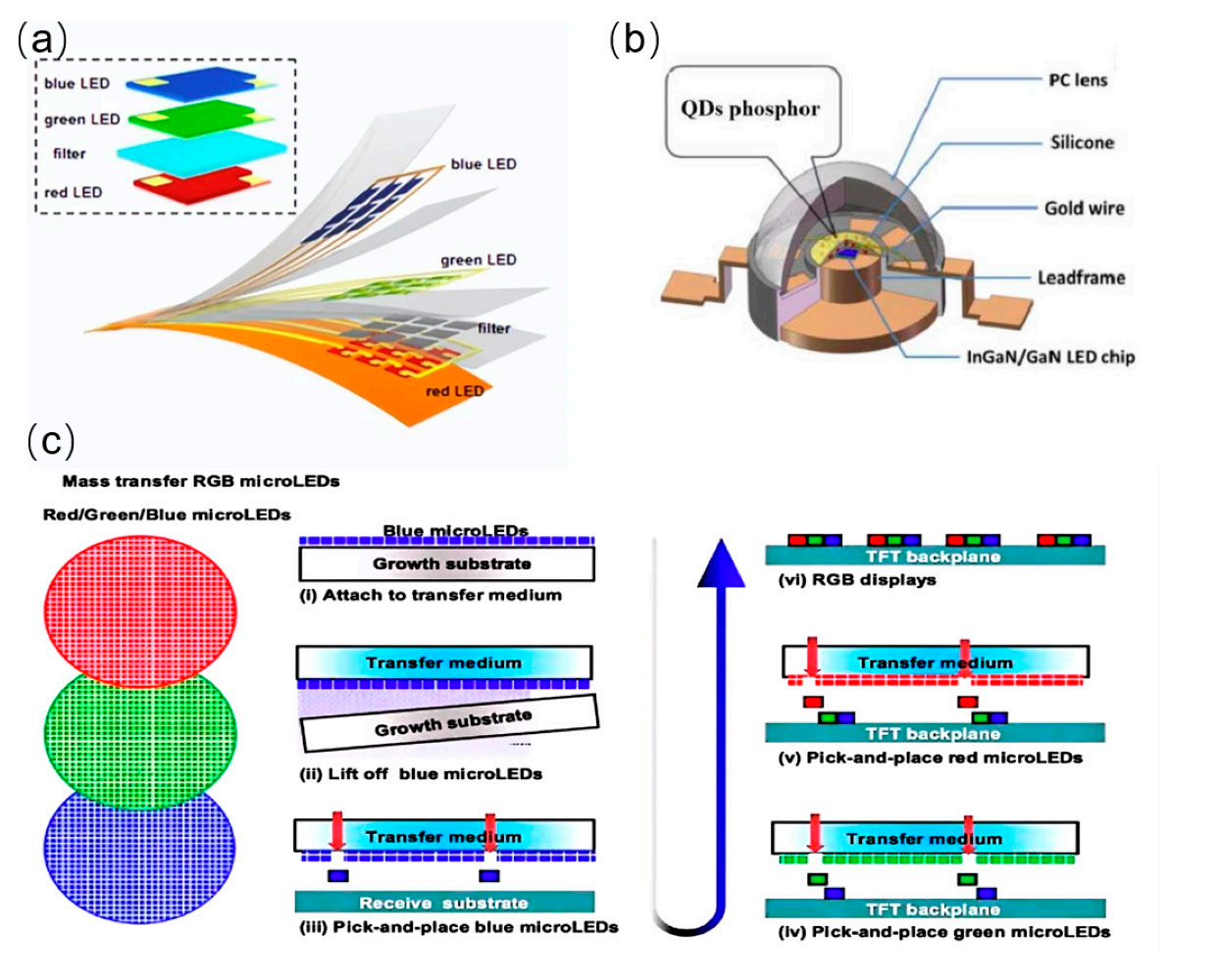
Figure 2. (a) $chem atic of three-color stacking technology. (b) Schematic of a light-emitting quantum dot.(c)Schematic of mass transfer.
There are several ways to drive micro-LEDs, the most commonly used being TFT andCMOS driver circuits as shown in Figure 3. The discrete driver allows each micro-LED tobe individually controlled by driver circuits to achieve color, brightness, etc.

Figure 3. Development of micro-LED driver display
TFT driver circuit: The TFT (Thin-Film Transistor) driver circuit is an active matrix driver circuit commonly used in current displays. It is widely used in various types of flat panel displays, such as LCD TVs, laptop computer displays, mobile phone screens, and so on. The TFT driver circuit usually consists of a driver chip, a TFT array, and power/signal lines. The driver chip is the core part, receiving external signals and controlling the conduction and turn-off of the TFT . The TFT array works as a current switch to control the brightness and color of each pixel by changing the conduction state. The transistors are usually made of monocrystalline or polycrystalline silicon and have high current driving capability and low switching voltage. Power and signal circuits are used to provide power and transmit control signals. Multiple supply voltages and clock signals are usually required to ensure that the thin-film transistors operate properly.
2. Innovation and Development of On-Chip Integration Technology
Integration technology plays a vital role in micro-LED displof high-performance micro-LED displays. Here, it is important to obtain high performance in current, voltage, and signal power in GaN-based transistors. Integrated devices are more difficult to fabricate compared to individual devices, but the cost of manufacturing is not significantly higher when all modules are made on the single chip. Currently, on-chip integration still faces many challenges in micro-LED displays. For example, during the manufacturing process, a high-temperature treatment of ~800 ◦C is required to form Ohmic contacts, which would exceed the thermal budget of the LED device, resulting in a degradation of device performance. There are some difficulties and challenges in the process of integrating different transistors with micro-LEDs. Because micro-LEDs are very small, any tiny defect can cause the entire display to fail, so how to improve the yield rate is a challenge that needs to be solved. The transistors and micro-LEDs must be precisely matched in size to ensure that each micro-LED is properly controlled, which requires very precise equipment and processes. Although micro-LEDs are inherently more energy efficient, they can generate a lot of heat when operating at high brightness. Effective thermal management solutions are therefore required to prevent overheating from affecting the performance of the device. In order to enhance the reliability of integrated devices, researchers generally take some methods to improve the reliability of micro-LEDs, such as reducing the defect density of epitaxial growth, designing efficient device structures, and developing effective thermal management ay. Micro-LEDs offer higher injection current density, smaller pixel size, higher brightness, and longer lifetimes than conventional display. Therefore, integration technology is very critical for the development .
An ideal bipolar transistor (BJT) consists of two pn structures with different doping concentrations. In 2022, S. Hao et al. from Fuzhou University simulated a new type of lightemitting triode, as shown in Figure 4a. One GaN-based LED was vertically integrated with one npn-type BJT on the same chip, where the cathode of the LED and the collector of the BJT share the same n-GaN layer. This vertically integrated structure provides the ability of acquiring higher-resolution display compared to HEMT and MOSFET integration. The optical output power of the integrated device can be regulated by a smaller base-level current. The cut-off frequency can be raised up to 80 MHz and more. The luminous intensity is closely related to the frequency, amplitude, and duty cycle of the pulse signal, proving a stronger capability of controlling the device. However, there are still many difficulties in the process to be solved. The difference in epitaxial temperature and lattice mismatch between P-GaN and N-GaN will result in a poor device performance.
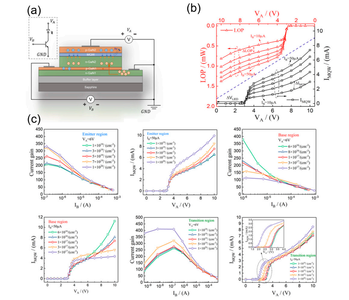
Figure 4. (a) Equivalent circuit and operating schematic of the device. (b) Output characteristics andoptical output power characteristics of the device. (e) Current gain and output characteristics fordifferent doping concentrations in the emitter, base, and transition regions.
As shown in Figure 5c, the integrated LEB]T with the larger emitter area exhibited alinear relationship between the peak EL, intensity with respect to the base current intensityunder the voltage of Vce = 5 V, demonstrating its electro-optical emitter-like function.Reduced emitter area can provide a higher current gain. An average current gain of 20 anda bandwidth of 180 MHz were obtained by nanorods array.
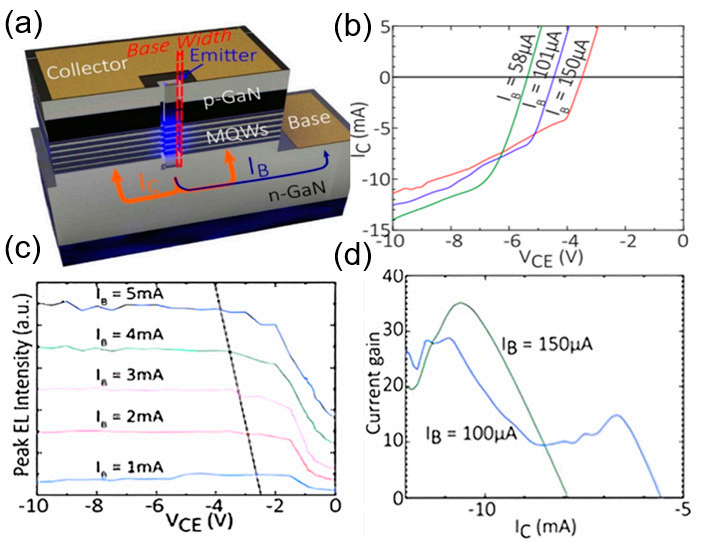
Figure 5. (a) 3D schematic of the device cross-section. (b) I-V characteristic curves of the emissionregion of the nanostructures. (e) EL, mapping of the monolithic BjT structure. (d) Curent gainextracted from the I-V curves
Overall, the BJT-integrated LED demonstrated some promising advantages such as a compact circuit, reduced power dissipation, and improved energy conversion efficiency by integrating BJTs and LEDs on the same chip. The BJTs acted as current amplifiers to provide precise current control and regulation, significantly reducing base current and providing a current gain of approximately 20 , resulting in a good driving and dimming control. Vertically on-chip-integrated BJTs and LEDs can achieve larger device scale and higher resolution and might be one of the solutions for high-brightness and high-resolution display scenarios. However, there are still some problems to be solved. The fabrication of BJT-integrated structures is complex, requiring a special growth process and microfabrication technical support, which greatly increases the manufacturing cost and reducesyield. The device size and electrical characteristics of BjIs and LEDs need to be carefullydesigned and accurately matched to avoid the current mismatch and power loss. The B]Tintegrated micro-LED technique is expected to prmote the integration and support for thedevelopmentofdisplay technology and visible light communication.
In 2014,a research team from National Taiwan Normal University fabricatedMOSFET structures on exposed GaN layers, and connected LEDs in series as depicted inFigure 6a. An LED structure was grwn on 2-inch sapphire substrates using a low-pressuremetal-organic chemical vapor deposition system. The LED structure was then selectivelyremoved by dry etching (ICP) with Ar/Cl, mixed gases to expose the n-type GaN layer forthe subsequent fabrication of MOSFET, Then, an n-type GaN layer on top ofthe MOSFETmesa was patterned by standard photolithography and ICP dry etching to give a filmof 150 nm for the current channel. The monolithically integrated MOSFET devicesdemonstrated excellent current injection capabilities and were capable of modulating thebrightness of the LED by controlling the gate voltage. As can be seen from Figure 6b, thelight output power of the LED rapidly increased at low injection currents (less than 20 mAand reached saturation at higher injection currents (greater than 90 mA). In 2016, Xing Luand colleagues from the South China University of Technology fabricated an integrateddevice combining MOSFET with an LED as shown in Figure 7a [41], where they grewp-GaN and n-GaN on top of the LED to realize a p-n-p MOSFET structure. In the processof fabricating the MOSFET, tetramethylammonium hydroxide (T'MAH) was employedto repair the sidewall damages of the MOSFET, thereby enhancing its electron mobilityand achieving a high output current density exceeding 1.4 kA/m'. The TMAH wet etchwas found to be effective in removing damage from the dry-etched GaN sidewall TheI-V characteristic of integrated device indicates that the turn-on voltage is 3 V, and theon-resistance is 4.1 m(.cm. Under a forward injection current of 20 mA, the voltage olLED is only 3.72 V, The LED device exhibits a light output power (LOP) of 16 mW and apeak external quantum efficiency (EQE) reaching up to 33%.
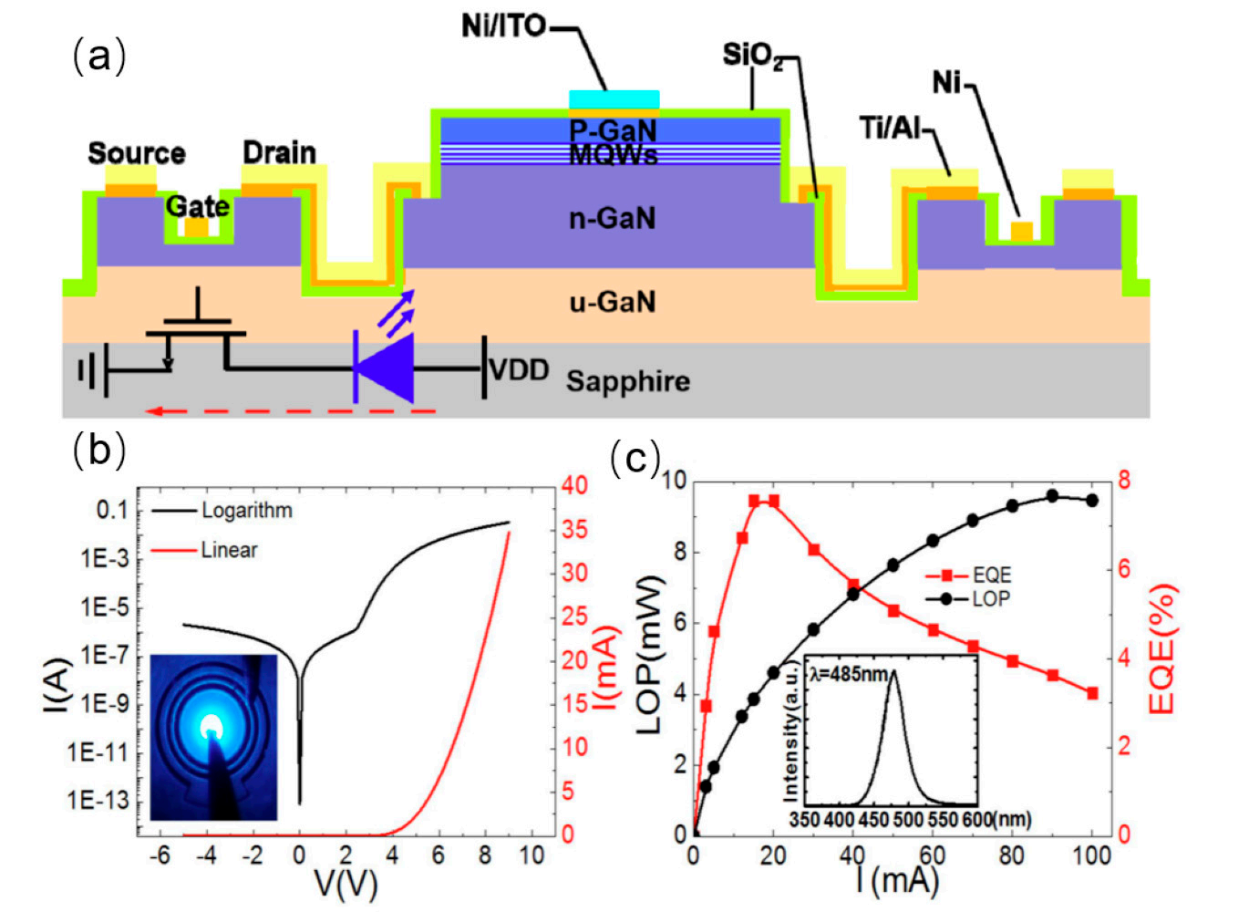
Figure 6. (a) $chematic of the MOSFET--LED integrated device and equivalent circuit. (b) I-V charac.teristic curve and picture of illumination under 20 mA current injection. (e) LOP and EOE of theintegrated device and EL mapping under 20 mA current injection .
3. Conclusions
Overall, the on-chip integration technology of micro-LEDs with driving circuits has made significant breakthroughs. In comparison to traditional methods such as mass transfer and bonding techniques, the novel approach of integrating drivers and display elements on a single chip demonstrates numerous advantages. The drop in threshold voltage from 2.9 to 0.8 V represents a significant reduction in power consumption. The increase in carrier mobility from 10.5 to 1810 cm2/(V·S) means a faster response frequency. Furthermore, monolithic integration technology not only plays a vital role in the display domain but also holds immense potential in various other fields, including visible light communication and chip-level optical interconnection. It is believed that through the efforts of an increasing number of researchers, the performance of integrated devices will be further enhanced, device structures will become more streamlined, and functionalities will grow more diverse. In the near future, on-chip integration technology is proposed to have broader application prospects within the realm of micro-LED displays.
下一篇: 氮化镓衬底化学机械抛光新技术