As the representative of substrate material, gallium nitride (GaN) has excellent mechanical properties and high thermal stability. Achieving high surface flatness is critical for subsequent epitaxial growth and device fabrication processes. Chemical mechanical polishing (CMP) technique of GaN is commonly one of the most effective ways to achieve atomically smooth surfaces. However, the current process is difficult to meet the needs of industrial development due to the characteristics of low material removal rate. Assisted enhanced CMP technique is deemed to possess significant potential due to its improved processing efficiency and surface topography quality. Herein, a variety of auxiliary enhanced CMP systems are designed and studied. In this review, recent advances both in conventional and assisted enhanced CMP of GaN are comprehensive presented, with a focus on their potential applications in various fields. The mechanism and design strategy of the process are discussed and summarized. The key issues in machining atomically flattened surface are outlined, and future strategies for sustainable development are also proposed. This review provides a novel perspective on GaN processing and offers more inspiration for future research to realize its development and commercial application.
1. Introduction
Gallium nitride (GaN) crystals are considered to be one of the most promising third-generation semiconductor materials widely used in light-emitting diodes (LEDs), ultraviolet detectors, and other fields.Due to its exceptional physical and chemical properties, including outstanding mechanical strength, high thermal conductivity, remarkable radiation resistance, superior breakdown voltage, and stable chemical characteristics. However, the acid and alkali resistance, high hardness, and brittleness of GaN pose challenges in achieving high flatness and damagefree surface/subsurface through ultraprecision machining technologies. This difficulty has become an urgent global issue that also hampers the application prospects of GaN crystal components.
The key substrate developments of GaN can be categorized into two areas: i) bulk crystal growth techniques as substrates, and ii) substrate processing techniques to optimize the shape of bulk crystals. These are crucial for device growth and subsequent chip processing, playing a vital role in communication, display, lighting, and other fields.Significant progress has been achieved in the former area, as evidenced by recent reports.However, the development of post-processing technology lags behind that of crystal growth mainly due to the extremely challenging machinability of substrate manufacturing processes.
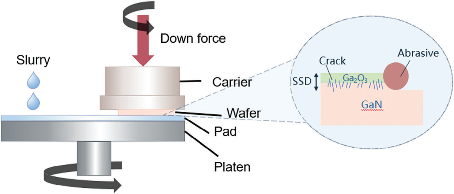
Traditional CMP is a polishing technique that employs alternating oxidation and mechanical polishing.As the final step in post-processing, it is considered the sole means of eliminating the SSD layer and surface scratches while enhancing surface topography to achieve atomically flat wafers.Its working mechanism can be summarized as follows: under certain pressure, Ga2O3 is formed on the surface of a GaN wafer through oxidation in a polishing liquid composed of ultrafine particles and chemical reagents.The mechanical grinding process, which involves rotating with the polishing pad, removes the surface oxides to produce a smooth and flat surface.
2. Various GaN CMP Technologies
The chemical mechanical polishing (CMP) technique was initially employed in 1992 for the purpose of refining silica in semiconductors. Subsequently, Tavernier et. al team provided a detailed account of the fine processing of GaN using CMP in 2002, and Tavernier’s team also the pioneers to employ colloidal SiO2 slurry for CMP on GaN. The working mechanism of traditional CMP as shown in Figure 1. Due to significant lattice and thermal mismatch between GaN and sapphire during growth, various defects are present in GaN crystals, including threading dislocation, edge dislocation, and mixed dislocation. Conventional CMP achieves surface smoothness by chemically oxidizing GaN with surface defects into Ga2O3 and mechanically removing the oxide layer. Therefore, conventional CMP treatment can effectively eliminate large surface defects and subsurface damages generated during the growth and processing of GaN wafers.The CMP process is employed to reduce the dislocation density and stress within the wafer caused by the mechanical polishing. Furthermore, the quality of epitaxial layers regenerated by CMP is superior to the as-grown state.This section mainly reviews the primary effect factors of traditional CMP, including polishing fluid and polishing CMP, including polishing fluid and polishing process.

Figure 1. The working mechanism of traditional CMP.
The composition and properties of polishing fluid play a decisive role in the polishing effect. GaN polishing solution is a crucial factor in the CMP process, significantly impacting the MMR and surface roughness Ra of GaN. Therefore, extensive research focuses on selecting each component and understanding their synergistic effects. The polishing fluid mainly contains abrasives, oxidants, surfactants and catalysts, and other key components. This section provides an overview of the polishing effect and mechanism of key components such as abrasives, oxidants, surfactants, and catalysts used in the GaN CMP polishing solution.
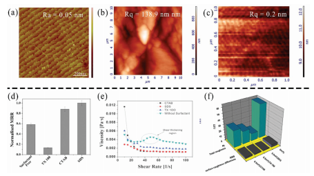
Lu et al. discovered that the addition of oxidant H2O2 to SiO2 abrasive resulted in an increase in its material removal rate (MRR) from 57.59 to 90.3 nm h−1 under identical conditions, while also improving its surface quality. The resulting surface roughness values were measured at 7 and 3.24 nm respectively after a polishing duration of 2 h using a polishing fluid. It was observed that the oxidizability increased with higher concentrations of H2O2. However, it should be noted that excessively high concentrations did not yield better results. More pits will appear when the H2O2 concentration is greater than 3%, which will increase the difficulty of removal. Due to the inherent instability of ·OH, it is prone to failure during the CMP process, resulting in reduced oxidation and polishing efficiency. In 2017, Pan et al.introduced a novel oxidant S2O8 2− with a higher electrode potential E0 = +2.5 = +2.5 – +3.1 V, longer half-life (≈4 s), and wider pH range (≈2–10) compared to ·OH (<1 μs). Consequently, this new oxidant exhibits a similar oxidation capacity as ·OH but offers an extended reaction time with GaN surface. The results indicate that, with Fe2+ as the catalyst, the rate of MMR is 121.1 nm h−1 and the surface roughness Ra is 0.05 nm (Figure 2A).

Fig2
The material removal efficiency is directly influenced by the concentration of abrasives, which alters the coefficient of friction (COF).The MMR initially increases and then decreases as the abrasive concentration rises. When the reduction in concentration is low, an increase in slurry concentration leads to a greater number of abrasive particles involved in polishing, thereby enhancing mechanical action and increasing MMR. When the concentration of abrasive is excessively high, the slurry viscosity increases and fluidity deteriorates. This may result in a decrease in polishing fluid on the grinding disc and hinder oxidation of the GaN surface.An increase in abrasive concentration will enhance lubrication while reducing shear stress, ultimately leading to a decline in MMR.
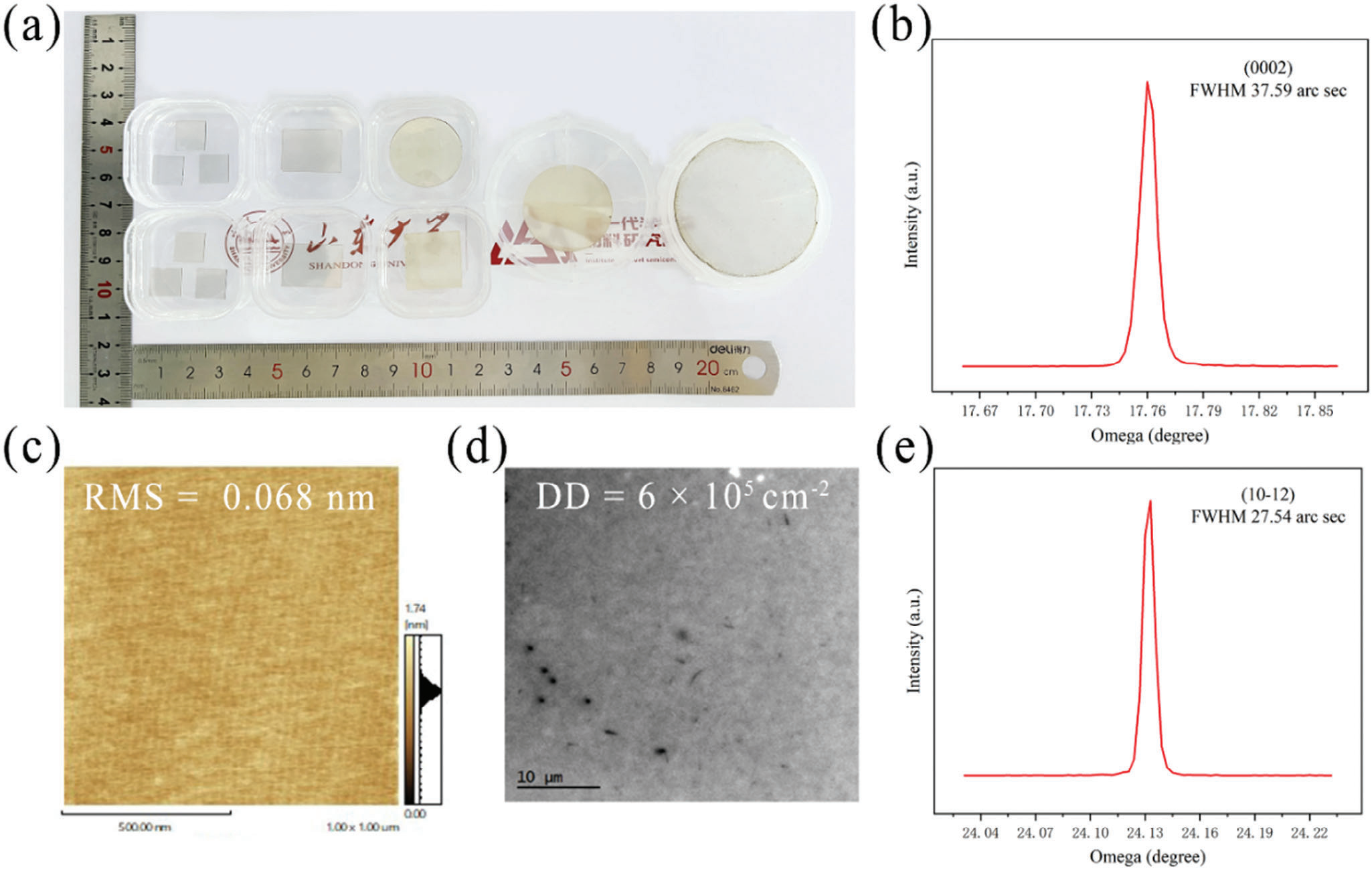
The State Key Laboratory of Crystal Materials at Shandong University has also conducted research on the growth and processing of GaN single crystals.This research team has overcome the key technology of homogeneous epitaxial growth of 2-inch single crystals by the HVPE method. Figure 3A. Aiming at the GaN single crystal substrate Ga surface processing difficulties and prone to sub-surface damage layer and other difficult problems, the systematic study of the different polishing liquid systems (acidic, alkaline, and neutral) on the Ga surface of GaN single crystal substrate polishing effect, to achieve the Ga surface scratches are removed, and sub-surface damage layer is also greatly improved, to obtain the surface roughness of 0.2 nm or less of the GaN single crystal substrate. Figure 3C. The processed samples are microscopically flat and have good crystal quality, with a half-peak width of 37.59 arcsec on the GaN single crystal (0002) face and 27.54 arcsec on the (10̄ 12) face, and dislocation densities as low as 6 × 105 cm−2. Figure 3B.D.E. For the specific research paper, a detailed report is to be made in the following.

Figure 3. A) Image of GaN wafers. B) (0002) surface high-resolution XRD pattern. C) AFM image RMS = 0.068 nm. D) CL image (dislocation density ≈6 × 105 cm−2) E) (10̄ 12) high-resolution XRD pattern.
Zhao et al. introduced purified terephthalic acid (PTA) into the H2O2 electrolyte as a buffering agent, thereby forming a protective film on the surface of GaN to mitigate surface corrosion. PTA exhibits remarkable corrosion inhibition capability, effectively mitigating or inhibiting excessive corrosion during electrochemical processes without significantly compromising subsequent polishing removal rates, resulting in a relatively smooth GaN surface. Through meticulous adjustment of the process parameters, the research group successfully obtained an optimal formulation consisting of a 4 wt.% H2O2 solution and a 10 mmol/L PTA solution. At this juncture, a harmonious synergy between the oxidant and corrosion inhibitor was achieved, leading to the formation of a uniform oxide layer and passivation film. The resulting optimal Ra value was measured at 0.74 nm.
4. Conclusion
Overall, this paper offers a comprehensive exploration of the recent advancements in traditional chemical mechanical polishing (CMP) and auxiliary CMP. The systematic analysis focuses on the influence of polishing fluid and process parameters on machining in traditional CMP. Additionally, the implementation of an assisted CMP strategy proves to be an effective approach for enhancing both GaN surface topography quality and material removal rate. The assisted system mainly focuses on adding optical, electrical, magnetic, and plasma to substantially improve the oxidation and mechanical removal capabilities. Since the oxidation rate is the controlling step in the polishing process, the introduction of auxiliary systems into conventional CMP can increase the oxidation rate of GaN wafer surfaces and facilitate chemical and mechanical interaction. Finally, we also discuss potential obstacles and opportunities for removing subsurface damage and achieving atomically smooth GaN wafer surfaces. This review provides novel research perspectives on GaN processing and provides additional inspiration for future research to advance its development and commercial applications.