AlGaInAs/InP material system's unique properties, such as a larger conduction band discontinuity (ΔEc = 0.72ΔEg) and a smaller valance band discontinuity have made it an attractive choice for photonic integrated circuits (PIC) devices. In this thesis, several novel PIC devices have been designed, fabricated, and characterized based on conventional 1550 nm AlGaInAs/InP multiple quantum well (MQW) laser diode (LD) epilayer structure.
The third device presented is the eight-channel electroabsorption modulated lasers (EMLs) array based on sidewall four phase-shifted sampled Bragg gratings(4PS-SBG), a C-band eight-channel EML array is presented, with a channel spacing of 0.8 nm. The use of 4PS-SBG sidewall DFB lasers can preserve high coupling coefficients (0.9 times of continuous uniform gratings) and maintain precise channel spacing control, significantly simplifying the EML device fabrication process, requiring only one metalorganic vapor-phase epitaxy (MOVPE) step and one III-V material etch. The DFB lasers exhibit side mode suppression ratios (SMSRs) greater than 42 dB, while the integrated EAM achieves a 20 dB extinction ratio (ER), and the 3-dB modulation bandwidth is more than 20 GHz.
By the way, I have designed, optimized, and fabricated two innovative InP-based devices: the 1D and 2D topological photonic crystal lasers. However, further optimization of the fabrication processes is required to ensure the functionality of these two devices.
1.1 InP-based Photonic Integration
The development opportunities for optical communication technology have emerged with the growing demand for communication bandwidth in modern society. While optical communication technology holds an absolute advantage in long-distance communication, the lack of popularity of optical communication devices at the user end makes it crucial to enhance device integration and reduce costs. Optical devices form the foundation and core of optical communication systems, representing a country's level of proficiency and capability in the field of optical communication technology.
Photonics Integrated Circuits (PICs) encompass the technology that seamlessly integrates multiple optical devices. Contrasted with conventional discrete components, PICs deliver notable advantages in size, energy efficiency, cost-effectiveness, and reliability. They signify the prevailing trajectory for advancing optical device technology into the future.
The novel Photonic Integrated Circuits (PICs) of alloys of III-V quaternary material system (AlGaInAs/InP or InGaAsP/InP) currently enable the generation, manipulation, and detection of optical signals. This has dictated the wavelength range of interest to the near-infrared region, where the bandgap of InGaAsP/ AlGaInAs can be adjusted, it can act as a transparent, absorbing, or light-generating material, while maintaining lattice matching with InP. The components in PICs, depending on the different material properties, can be defined into two domains: passive components, in which the material has a much larger bandgap than the propagating photon energy. Such as optical waveguides, multimode interference (MMI) couplers, AWG multiplexers, Mach-Zehnder modulators (MZMs) , as shown in Fig.1.1.1. Active components, using a material with a bandgap that is equal to or smaller than the energy of the propagating photons, such as semiconductor lasersincluding the Fabry-Perot (FP) laser, distributed feedback (DFB) and distributed Bragg reflector (DBR) semiconductor lasers. To enhance the electro-optical conversion efficiency, the quantum wells (QWs) have been employed in the fabrication of semiconductor lasers. These QWs are created within semiconductors by placing a material layer between two layers of a material with a wider bandgap, i.e., quantum barrier (QB). This arrangement generates a potential well that can only support discrete energy values. Electrons in semiconductors tend to cluster in the lowest energy levels, improving the efficiency of electro-optical energy conversion.

Figure 1.1.1 Several passive InP-based PIC components. (a) MMI couplers, (b) AWG multiplexers , (c) MZM
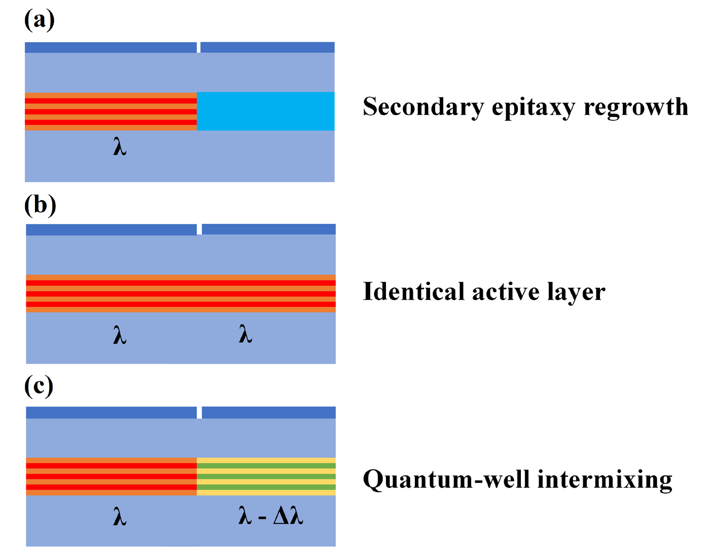
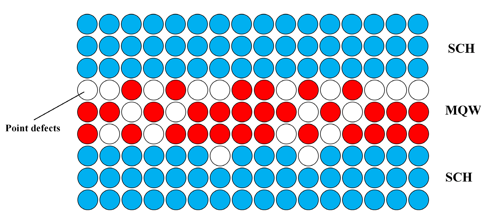
To integrate the passive components with the active source, several active/passive integration scheme techniques have been proposed based on the InP platform shown in Fig 1.1.2: first is the secondary epitaxy regrowth technique such as offset quantum-well waveguides, butt-joint regrowth, selective area regrowth . As the name suggests, those techniques require multiple rounds of metalorganic vapor-phase epitaxy (MOVPE) growth for the passive material to achieve compatibility with the active area. This approach allows for independent optimization of the performance of passive and active components, without needing to consider the compatibility of different epitaxial layers. However, a significant drawback of this technique is the necessity for a flawless joint interface to minimize scattering loss and enhance coupling efficiency. Additionally, the need for extra epitaxy growth can increase the overall cost of device fabrication. Other techniques without secondary epitaxy regrowth are identical active layer (IEL) and quantum-well intermixing (QWI). IEL means the passive device shares the same epitaxy structure as the active device, which is its greatest advantage and the greatest challenge either. QWI is a technique that selectively tunes the bandgap of the quantum well across a wafer post-growth. After intermixing, the MQW structure has similar characteristics to those of a bulk layer, and its material anisotropy disappears. The QWI involves a growth post-processing method comprising three main steps. Firstly, a large number of point defects are generated on the surface layer above the MQW layer. Secondly, under specific conditions, such as Rapid Thermal Annealing (RTA), the point defects move towards the quantum well region as shown in Fig 1.1.3. Lastly, the point defects cause intermixing of the component atoms of the quantum well/barrier material at the interface, resulting in a change in the material components and band gap wavelength.

Figure 1.1.2 Several InP-based active/passive integration approaches (a) secondary epitaxy regrowth, (b) identical active layer, (c) quantum-well intermixing

Figure 1.1.3 Defect diffusions during RTA in a QWI process.
There are various approaches to achieve QWI based on different methods for generating point defects. These include impurity-free vacancy diffusion (IFVD) [13], photo-absorption induced intermixing (PAID) , ion implantation-induced disordering (IIID) , and low-temperature growth induced intermixing in InP. To define different regions of the PIC device, a protective technique is usually employed to create a certain concentration of point defects in the selected region on the epitaxial wafer, while other areas have no point defects. After the RTA process, which promotes point defect diffusion and induces intermixing between QW and QB, bulk-like materials with blueshift bandgap wavelengths are formed in designated regions. The main advantage of QWI technology is that it uses traditional planar epitaxial growth technology and does not require additional growth processes. However, due to the lateral movement of point defects during their generation and diffusion, the composition transition between different materials is not steep, and there is a composition transition region of 2-3 μm, which usually has little effect on the performance of the integrated photonics device.
Within the InP platform, a plethora of PIC devices cater to optical communication needs. This section provides an overview of two key photonics devices: semiconductor lasers and polarization controllers.
上一篇: 氮化镓衬底化学机械抛光新技术
下一篇: 溅射沉积Ga2O3薄膜的微结构和光学特性