ABSTRACT
Semiconductor materials have played a huge role in advancing today’s technology through the electronic and photonic devices ushered in over the years. The advancement has been driven in part by society’s growing need for electronic devices capable of handling higher power, higher temperature, and higher frequency. Current research efforts are expanding to ultra-wide bandgap semiconductors such as gallium oxide (Ga2O3). The principal goal of this dissertation is to obtain high quality β-Ga2O3 films with controlled conductivity by magnetron sputtering deposition. The specific objectives are the following: To grow β-Ga2O3 films on sapphire substrates (section 5.2) and on native β-Ga2O3 by rf sputtering (section 5.3), to produce doped and undoped β-Ga2O3 films (Section 5.4). Additionally, to grow Lu2O3/ Ga2O3 and B2O3/Ga2O3 alloy films on (2 0 1) UID or Sn-doped Ga2O3 and Al2O3 substrates to tune Ga2O3 original bandgap (Section 5.5). To obtain microstructural, morphological, compositional, and optical data from XRD, AFM, SEM, EDS, and UV-Vis characterization methods for all the experiments mentioned above. From this data, correlate the effects of the varying parameters for the optimization of the films, to use the developed films to fabricate Schottky barrier diodes and proceed with the electrical characterization of the fabricated devices (section 5.6).
Currently, 40% of the total primary energy consumption in the United States is attributable to electrical energy. Power electronics play a key role in the conversion of the electrical energy produced in power plants by reducing the high voltage generated to one that can utilize. Approximately 30% of total electrical energy currently flows through power electronics, with projections indicating a substantial increase to possibly reach 80% over the next decade. In modern systems, this conversion is performed by the switching and rectifying characteristics of semiconductor devices such as diodes, thyristors, and power transistors. When the electrical energy passes through these components, it inherently experiences an energy loss, creating an opening for researchers to introduce new materials with enhanced properties leading to high conversion efficiency. The power conversion sector is expected to expand from $52 billion to $71 billion by 2023, driven by the increasing consumption of electrical energy. Figure 1.1 depicts a schematic highlighting the significance of power electronics in the process of power conversion, especially considering that since 30% of the total energy in the form of electricity passes through power electronics.
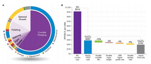
Wide-bandgap (WBG) materials such as silicon carbide (SiC) and gallium nitride (GaN) have been used in ultrahigh-voltage power switching applications as a better alternative to Si. These WBG SiC and GaN semiconductors can tolerate a much higher breakdown electric field (Ec) at a comparable dielectric constant (ε) and similar charge carrier mobility (μ), which translates into a larger figure of merit (BFOM=εμEc 3 ), compared to Si. One of the main downsides of these materials is the higher cost of the single crystal substrate wafer production, due to the complexity of the crystal growth chemistry and the smaller scale of the crystal growth industry. Researchers worldwide have extensively explored semiconducting metal oxides due to their appealing attributes, including exceptional transparency, wide band gap, and their applicability in power electronic devices. High-quality gallium oxide (Ga2O3) wafers can be fabricated using simple metal-based crystal growth processes used in the fabrication of inexpensive Si or sapphire (Al2O3) crystals. Furthermore, epitaxial growth of high quality Ga2O3 thin films has been demonstrated by various methods including chemical vapor deposition, pulsed lased deposition, molecular beam epitaxy, metal-organic chemical vapor deposition and magnetron sputtering. Among the different fabrication methods for depositing oxide thin films, magnetron sputtering is the preferred method in many industrial processes because it is an established technique, suitable for large area fabrication and roll-to-roll processing. The advancing Ga2O3 based power electronic technology has the potential to address the trade-off between cost and performance effectively by offering an enhanced performance at a lower cost. Figure 1.2 shows the results of techno-economic modeling for 6 in wafers and indicates that the cost of wafers will drop significantly in the future as more large-size and high-volume manufacturing processes are introduced.

Figure 1.2 (a) Modeled Ga2O3 wafer manufacturing cost as a function of the fabrication process step (inner circle) and cost type (outer ring). The total cost is dominated by Iridium (Ir) material used in Ga2O3 crystal growth crucible. (b) Modeled 6 in wafer costs comparison for Ga2O3 and SiC wafers, and the Ga2O3 cost reduction potential. The Ga2O3 cost is >3x less compared to SiC and can be further reduced by better iridium (Ir) crucible utilization and faster polishing and epitaxy processes.
This dissertation focuses on gallium oxide semiconductor materials, specifically the thermodynamically stable polymorph of monoclinic, β-Gallium Oxide (β-Ga2O3). The unique properties of β-Ga2O3 make it a promising material for a new generation of power and optoelectronic devices. Due to its wide bandgap (4.9 eV), high transparency, and thermal stability, β-Ga2O3 has been of primary interest for use in power devices, solar-blind UV photodetectors, photocatalysts, gas sensors, solar cells, as well as phosphor, and transparent conducting films for electrodes on many optoelectronic devices. Controlled growth and characterization of the properties of the new material is a necessary step in bringing the material into use. As our understanding of gallium oxide’s properties improves, it has the potential to replace them in various applications, provided certain limitations can be addressed.
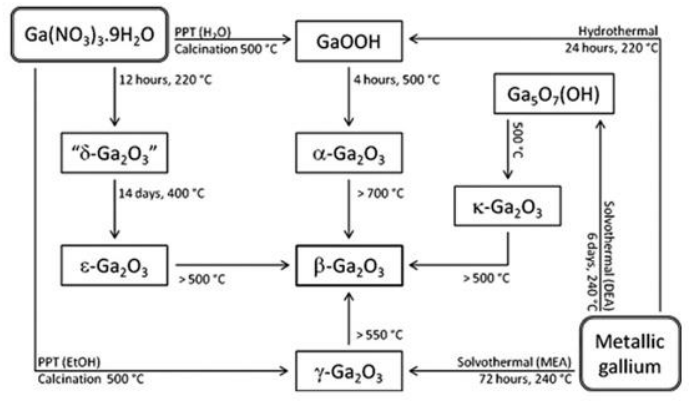
At least five different polymorphs (forms) of Ga2O3 have been reported, namely, rhombohedral (α), monoclinic (β), defective spinel (γ), cubic (δ), and orthorhombic (ε) structures, and a transient κ- Ga2O3. Of all its polymorphs, the β-Ga2O3 structure has shown to be the most stable under normal conditions of temperature and pressure. The other polymorphs can be either conductors or insulators, depending on the growth conditions, and will transform to the β- phase at sufficiently high temperatures up to its melting point 1900℃. These polymorphs not only differ in their crystal space, but also in their coordination number for Ga ions, and can be synthesized under specific conditions of pressure and temperature. For instance, the α-phase is rhombohedral with space group R3̅c, and can be obtained at temperatures of 1000 C and pressures of 4.4 GPa. The β-phase, which holds a monoclinic structure with space group C2/m, can be obtained from any other polymorph by heat treatment (Fig. 1.3) in air at sufficiently high temperatures ranging from 500-700 ℃.

Figure 1.3 Summary of the synthesis and interconversion of the polymorphs of Ga2O3 and related phases. Depending on the initial phase, temperatures in the range of 500-700 C are sufficient to allow a transformation to the β-phase.
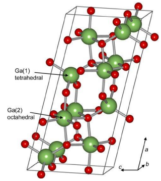
Crystallographic studies performed by Ahman et al, indicate that the unit cell of β-Ga2O3 contains two inequivalent Ga positions, one with tetrahedral geometry Ga (I) and the second with octahedral geometry Ga (II). The oxygen atoms are located three distinct positions labeled as O (I), O (II), and O (III), forming a distorted cubic closed-packed structure (Fig. 1.4). One oxygen atom is coordinated tetrahedrally, and the remaining two oxygen atoms are coordinated in a trigonal manner. A summary of the properties for all polymorphs is presented in Table 1.1.

Figure 1.4 Monoclinic crystal structure of β-Ga2O3
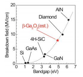
Gallium oxide is known to be an ultra-wide bandgap semiconductor, with an energy gap of about 4.7-4.9 eV. A semiconductor with a ultra-wide energy bandgap has a higher electric breakdown field, therefore Ga2O3 (8 MV/cm) has an electric field value higher than that of other commonly used semiconductors, such as Si (0.3 MV/cm), 4H-SiC (2.2 MV/cm) and GaN (2.0 MV/cm) as shown in Fig. 1.5.

Figure 1.5 Electric field vs Bandgap
Due to its wide band gap, pure stoichiometric β-Ga2O3 is colorless and transparent over a wide optical range, covering visible down to the UV-C (250 nm) region. These optical and electrical characteristics place β-Ga2O3 into the realm of transparent conductive oxides (TCOs). In addition, a strong correlation between electrical conductivity and absorption of the films have been reported. The electrical conductivity of the films is not only affected by the doping concentration, but also by the atmosphere in which the film is grown. Films grown in an oxidizing atmosphere are highly insulating and show a transparent or yellowish coloration, which is indicative of absorption in the blue range of visible light. In the other hand, films grown in reducing atmosphere are conductive and show more of a blueish coloration. This can be explained by the high density of dopants making the material absorb in the red and NIR regions of the spectrum.