Introduction

Pattern Transfer
For microsystems fabrication etch is a process that removes select materials from
the wafer's surface,
below the wafer's surface
from within the substrate.
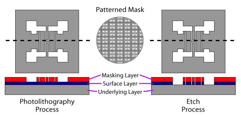
The etch process normally follows photolithography or deposition during which a protective masking layer is applied to the wafer's surface. The protective masking layer is used to identify the material to be etched and to protect material that is to remain. The previous figure labeled “Pattern Transfer,” illustrates a mask pattern transferred into a photosensitive layer, shown in red (masking layer), on the wafer's surface (Photolithography Process). During the Etch Process (right), that pattern is transferred into the surface layer, removing exposed areas of the surface layer and leaving areas in the underlying layer open to a subsequent process step.
In microsystems fabrication, the etch process is also used to remove material from underneath a layer or from the backside of the wafer. The graphic to the right illustrates both of these etch processes. In the top graphic (bulk back-etch), the silicon substrate has been selectively removed from the wafer's backside. In the bottom graphic (bulk front-etch), silicon substrate has been removed from underneath a film on the wafer's surface.
A combination of these etch processes allow for the construction of electronic and mechanical devices on the same microchip. These graphics also show the electronics (on-chip circuitry) on the same chip as the mechanical component (diaphragm/beam).

[Graphic courtesy of Khalil Najafi, University of Michigan]
In this unit, you will receive an overview of the two main methods of etching, referred to as wet and dry etch processes. You will also become familiar with the thin films that are etched in the construction of microsystems, and the corresponding etchants (chemicals) used.
The Etch Process for Microsystems

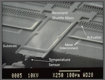
Layers of Micromachined Scanning Thermal Profilometer
[SEM courtesy of Khalil Najafi, University of Michigan]
Microsystems are three-dimensional devices consisting of several thin layers of materials. Each layer is designed to serve a specific role in the system's functionality. A layer may be used as
part of an electronic circuit (insulator or conductor),
a structural device for a mechanical component,
a transducer layer for sensors or
a sacrificial layer for devices such as cantilevers, diaphragms or beams.
Surface Etch

When building the electronics for a microsystem and for outlining mechanical components, the goal of the etch process is the same as that for building integrated circuits:
Remove selected regions on one layer (the surface layer) of the wafer to create either a structural pattern or to expose an underlying layer of a different material.
For electronic circuits, the underlying layer is now available for conductive interconnects. Connections between different conductive layers can be completed. For mechanical components, the surface layer is now patterned with specific shapes for structural components such as cantilevers, mirrors, or probes. The exposed underlying layer can also allow one to anchor a mechanical structure to it. Mechanical elements can also be conductive as in the case of electrodes or cantilevers.
Transistor etching

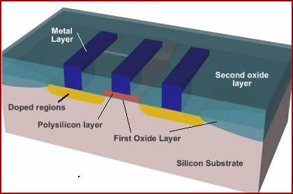
Etched layers of a transistor
[Graphic courtesy of Khalil Najafi, University of Michigan]
This graphic illustrates five etched layers which make up the construction of a simple transistor.
1. The first layer is the silicon substrate.
2. A layer of insulating oxide is deposited on the substrate and openings are etched for the doped regions.
3. A polysilicon layer is deposited and then etched to leave just a small portion for the transistor gate.
4. A second oxide layer is deposited and etched to provide openings for the metal contacts to the doped regions and gate.
5. A metal layer is deposited and etched to form the surface contacts.