Abstract
The quality of silicon carbide (SiC)substrates has great influence on the quality of the epitaxial layers atop. During the epitaxial growth, crystallographic defects and substrate contaminations may transform to various surface defects, such as carrots, polytype inclusions and scratches, which are detrimental to the performance and reliability of SiC devices. In general, chemical mechanical polishing (CMP) and post-CMP cleaning are the last two steps before the epitaxial growth, playing critical roles in controlling the scratch and contamination levels on the SiC substrates. In this article, the methods for reducing the aluminum (Al) and manganese (Mn) metal contaminations as well as other surface particle contaminations are investigated. We found that different commercial CMP slurries may lead to different contamination levels. Most importantly, by adding a scrubber cleaning step prior to the conventional RCA cleaning process, the contamination levels can be greatly reduced, achieving the quality for mass production.
1. Introduction
Advantages of wide bandgap semiconductors for fabricating the power devices have been widely discussed. Particularly, silicon carbide (SiC)with high breakdown electric field (2.5 MV cm−1 versus 0.3 MV cm−1 for Si) and high thermal conductivity (270 W m−1 K−1 versus 150 W m−1 K−1 for Si) have been considered as the most promising semiconductor to be used in the traction inverters of electric vehicles(EVs), especially when the EV battery voltage is increased from 400 V to 800 V, for the sake of fast charging and high power density. Despite the strong market demand mainly driven by the EVs, the production of SiC substrates by using the physical vapor transport (PVT) method remains slow. In general, it takes 5 to 10 days to obtain a SiC boule with about 1.5 to 3 cm thick [5]. Subsequently, the SiC boule needs to go through cropping/blocking, creating flat/ notch, slicing, edge grinding, laser marking, lapping, grinding, CMP, post-CMP cleaning, inspecting and packaging to yield 10 to 20 pieces of epitaxy-ready SiC substrates.
Among the process mentioned above, the CMP and post-CMP cleaning steps play a critical role in preventing the wafer losses due to unaccepted surface roughness, surface scratches and contaminations. In general, angstrom-level flat SiC substrates can be obtained by the CMP process, which involves oxidation of the SiC surface (figure 1(A)), followed by removal of the oxide layer by slurry abrasives and pads(figure 1(B)). The cycle of oxide growth and removal can effectively remove the machinery marks and subsurface damages, which are formed during the prior steps of mechanical lapping and grinding. Various types of CMP abrasives have been developed to optimize the CMP condition, such as single material abrasive, mixed material abrasive and core–shell abrasive. However, the abrasive residues and other CMP byproducts might be either mechanically-embedded or chemically-bonded to the SiC substrate surface at the end of the CMP process, resulting in surface contaminations. This occurs during the time, typically a few seconds, when the SiC wafer remains soaking in the slurry environment before the polishing head is removed from the polishing platen for unloading the wafer(figures 1(C) and (D)). To resolve this issue, the post-CMP cleaning is necessary to remove organic, metallic and abrasive contaminations caused by the CMP. Maintaining minimal contamination levels is also critical for achieving high quality epitaxial growth. Therefore, the CMP and post-CMP cleaning steps are complementary to each other. A well integration of both parts can effectively increase the wafering yield, so that the maximum epitaxy-ready SiC substrates per boule can be achieved.
For the traditional post-CMP cleaning methods, such as RCA cleaning and sulfuric peroxide mix (SPM) cleaning, the working principle is chemical oxidation followed by etching. This approach becomes problematic for SiC due to its chemical inertness, and the detailed cleaning mechanism on the SiC surface has yet to be explored. This paper presents a process integration method by selecting relatively easy-to-clean commercial CMP slurry to facilitate the post-CMP cleaning. Furthermore, a scrubber mechanical cleaning step is added between the CMP and RCA cleaning steps for minimizing the contamination levels and achieving the quality for mass production.
2. Experimental section
Prime grade, 150 mm diameter, N-type, as-grinded 4H-SiC wafers were purchased from a commercial supplier. In a class 1000 clean room, a batch type single-side CMP system was used in this study. As shown in figure 2, the CMP system comprises the followings: (1) Four active carriers with adjustable down force and rotation speed. Each carrier can load three of 150 mm SiC wafers. (2) A template mounted on the carrier that fixes the wafers in its 3 pockets. The pocket depth is about 2/3 of the wafer thickness. (3)A grooved polyurethane (PU) polishing pad with 920 mm diameter. The PU pad is conditioned by a diamond disk for providing a stable mechanical force that can prevent the noise of haze and scratches from affecting the optical inspection in this study. (4) A stainless steel platen with adjustable rotation speed on which the PU polishing pad is mounted. The platen can provide a datum plane to control the wafer surface geometry during the CMP process. The product of down force and rotation speed as a function of the CMP process time is shown in figure 3. In the first few minutes, a pre-polishing step with lower down force and rotation speed is applied to stabilize the system (Zone 1). Then, the down force and rotation speed quickly ramp up to enter into the main polishing process, during which a well balance between the removal rate and wafer flatness is achieved (Zone 2). Subsequently, a deionized water(DIW) polishing step follows, during which only DIW is supplied into the environment and the down force and rotation speed are kept low for removing the contaminations and slowing down the chemical reactions(Zone 3). Finally, it takes a few seconds to raise the polishing head and unload the wafers(Zone 4). This corresponds to figure 1(C), when the remaining abrasive residues and other CMP byproducts could be either mechanicallyembedded or chemically-bonded onto the SiC substrate surface. In this work, the down force was typically between 2 and 5 psi and the rotation speed between 40 and 80 rpm. Furthermore, two types of commercial CMP slurries were used in this study. The slurry A is composed of Al2O3 particles(1 to 2 wt%)with the pH = 9 and the slurry B is composed of core–shell Al2O3 particles(1 to 2 wt%)with the pH = 4. Both slurries contain the potassium permanganate (KMnO4) oxidants(1 to 2 wt%). The SiC removal depth was controlled to be 2 μm on Si-face and C-face surfaces for both types of the slurries. Furthermore, the C-face was polished prior to the Siface for preventing extra contamination on the Si-face. The material removal amount was measured by the SiC weight loss before and after the CMP process.

Figure 1.Illustrations of the CMP process, including (A) formation of an oxide layer on the SiC substrate surface by the oxidant (e.g. KMnO4) in the CMP slurry, (B)removal of the oxide layer by the abrasives and polishing pad under appropriate down force and rotation speed, and (C) SiC wafer remaining soaked in the CMP slurry before the polishing head is removed from the polishing platen for unloading the wafer. (D) Abrasive residues and other CMP byproducts could be either mechanically-embedded or chemicallybonded onto the SiC substrate surface, resulting in surface contaminations.
All the test wafers were kept in a DIW tank when transferred from the CMP step to the post-CMP cleaning step. In a class 100 clean room, a stand-alone single-side brush cleaning station for the scrubber cleaning and a RCA cleaner were used. The RCA cleaner consists of six sequential tanks, including an overflow tank, a SC1 tank (NH4OH / H2O2 / DIW), a quick drain rinse (QDR) tank, a SC2 tank (HCl / H2O2 / DIW), a QDR tank and an overflow tank. After the post-CMP cleaning, the SiC wafers were spin-dried and packaged in new cassettes for preventing extra environmental contaminations. For evaluating the contamination levels on the SiC wafer surface, two inspection tools were used in this study. The first one is Candela CS920 from KLA-Tencor Corporation, which combines five complementary imaging modalities, including dark field, bright field, slope, phase and photoluminescence, for detecting the crystal defects, particles and scratches, respectively. The second one is ICP-MS 7900 from Agilent Technologies, which analyzes the metal concentrations in the HF + H2O2 solution collected from the Si-face surface of the post-CMP cleaned SiC wafer. In this study, we focus on the aluminum (Al) and manganese (Mn) metal levels, because they are the main contaminations from the abrasives and oxidants in the CMP slurry.

Figure 2. (A) Schematic diagram and (B) photograph of the batch type single-side CMP system.
3. Results and discussions
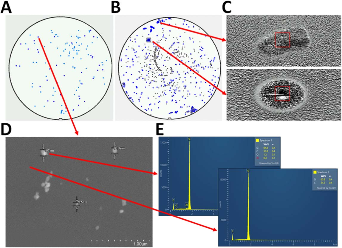
In general, the total defect count on the SiC substrate surface after the epitaxy is multiplied from that before the epitaxy. Therefore, it is critical to minimize the defect count, which mainly results from the abrasive contaminations, during the post-CMP cleaning step. Figures 4(A) and (B)show the Candela defect maps of the same SiC wafer as-polished and after epitaxy, respectively. Although the correlation of defect locations before and after epitaxy is ambiguous, the increase of defect counts is obvious. As shown in the SEM image of the aspolished SiC substrate (figure 4(D)), there are multiple particle contaminations detected at the location indicated by the red arrow in figure 4(A). The diameters of the particles range from 59.5 nm to 107 nm. By using energy-dispersive x-ray spectroscopy (EDS) element analysis(figure 4(E)), the composition of the particles is determined to be 64.6 wt% Si, 33.8 wt% C, 1.2 wt% O and 0.4 wt% Al, indicating that nanosized SiC debris can be generated as a CMP by-product and left on the substrate surface, in addition to the Al2O3 abrasive contaminations. In contrast, the composition of the substrate without contamination is 65.8 wt% Si and 34.2 wt% C, corresponding to pure SiC. Figure 4(C)shows the representative shapes of the surface defects on the SiC substrate after epitaxy.

Figure 4. (A) and (B)Candela defect maps for the same SiC substrate as-polished and after epitaxy. (C) Representative shapes of the surface defects on the SiC substrate after epitaxy.(D) SEM image of the as-polished SiC substruate.(E) EDS element analysis of the particle contaminations and the pure SiC substrate.
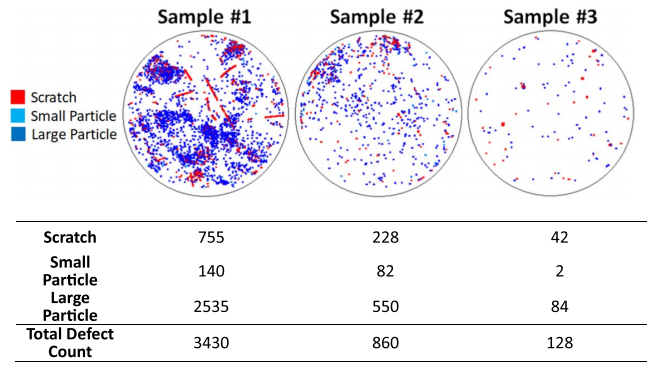
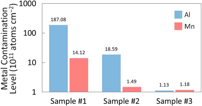
Next we investigate the methods for reducing the metal contaminations as well as other surface particle contaminations. The experimental design is summarized in table 1. We first compare the contamination levels of the SiC substrates using different commercial slurries for the CMP step (Sample #1 and #2). Then, by choosing the relatively easy-to-clean CMP slurry, we compare the contamination levels of the SiC substrates with and without the scrubber mechanical cleaning step before the final RCA cleaning (Sample #2 and #3). As shown in the Candela defect maps in figure 5, the scratch and particle counts of the SiC substrate using the slurry A (Sample #1) are much higher than using the slurry B (Sample #2). In general, the slurry conditions, such as viscosity, pH, purity and zeta potential between the particles and wafer surface, have great influence on the CMP outcome. Here, the slurry B leads to a much lower total defect count than the slurry A, likely because the acidic CMP condition in combination with the core–shell particle structure can help the Al2O3 abrasives better adhere to the SiC surface through electrostatic interactions. Besides, the abrasive shell can effectively inhibit chemical bonding to the SiC surface, thereby increasing the cleaning efficiency of the DIW polishing step (Zone 3 in figure 3). Furthermore, as indicated by the ICP-MS analysis in figure 6, the Al and Mn concentrations on the SiC substrate surface using the slurry A are much higher than using the slurry B, which is consistent with the Candela mapping result in figure 5. The Al and Mn are chosen for monitoring the abrasive (Al2O3 particles) and oxidant (KMnO4) contaminations. Nevertheless, neither Sample #1 nor #2 can meet the quality for mass production of epitaxy-ready SiC substrates. For further improvement, the scrubber mechanical cleaning step is added after the CMP and before the RCA cleaning (Sample #3). As shown in figures 5 and 6, the total particle count and the Al concentration of Sample #3 are greatly reduced from 860 to 128 (85% reduction) and from 18.59 × 10¹¹ atoms cm−2 to 1.13 × 10¹¹ atoms cm−2 (94% reduction), respectively. Although the DIW polishing step can remove most of the contaminations and slows down the chemical reactions(Zone 3 in figure 3), the remaining abrasive residues and other CMP byproducts can still contaminate the SiC surface during Zone 4 in figure 3. Owing to the chemical inertness of SiC, the RCA cleaning alone, whose working principle is based on oxidation of the contaminations followed by etching, cannot efficiently remove all abrasive and oxidant residues. In this regard, by adding the scrubber mechanical cleaning before the RCA cleaning, the contamination level that meets the quality for mass production can be achieved.

Figure 5.Candela defect maps for the SiC substrates treated with different CMP and post-CMP cleaning conditions as listed in table 1. Note that the particles on the SiC wafer surfaces with sizes less than 0.3 μm are classified as small particles and more than 0.3 μm as large particles.

Figure 6.ICP-MS concentrations of Al and Mn for the SiC substrates treated with different CMP and post-CMP cleaning conditions as listed in table 1.
4. Conclusions
In this paper, we first show that the total defect count of the same SiC substrate after epitaxy is multiplied from that before the epitaxy, pointing out the importance of post-CMP cleaning. The nanosized particle contaminations on the as-polished SiC substrate result from not only the Al2O3 abrasives but also the SiC debris as a CMP by-product. As revealed by the Candela defect maps and the ICP-MS concentrations of Al and Mn, which are chosen for monitoring the abrasive and oxidant residues, the slurry with core–shell Al2O3 particle structure and pH = 4 can lead to much lower scratch and particle counts than the slurry with pH = 9, indicating that the acidic CMP condition in combination with the core–shell structure can help the Al2O3 abrasives better adhere to the SiC surface through electrostatic interactions. Furthermore, the abrasive shell can effectively prevent the Al2O3 abrasives from being chemically-bonded to the SiC surface, thereby increasing the cleaning efficiency of the DIW polishing step. Most importantly, owing to the chemical inertness of SiC, the RCA cleaning alone cannot efficiently remove all abrasive and oxidant residues. In this regard, the scrubber mechanical cleaning step is added before the RCA cleaning, leading to 85% reduction in the total particle count and 94% reduction in the Al concentration. This paper presents a process integration method by selecting the relatively easy-to-clean commercial CMP slurry and adding the scrubber mechanical cleaning step before the RCA cleaning for achieving the quality for mass production of epitaxy-ready SiC substrates.
上一篇: 半导体湿法刻蚀概述