Abstract
In this work, nanostructured zinc sulfide (ZnS) thin films with different contents (2-10 at.%) of copper disulfide (Cu2S) were prepared by pulsed-laser deposition (PLD) method. The thin film samples with 2, 4 and 6 at.% of Cu2S showed that the ZnS thin films have wurtzite structure. The peak belonging to the Cu2S was observed on the xray diffraction patterns of the samples containing 8 and 10 at.% of Cu2S. Furthermore, the x-ray diffraction patterns of porous silicon showed a broadening in the FHWM with increasing etching time. A reduction in the average diameter of the particles with increasing etching time was observed according to the results of atomic force microscopy performed on the prepared samples. The photoluminescence spectra of the porous silicon samples showed that the etching time has a significant effect on the position of UV emission and a blue shift was observed as the etching time was increased from 10 to 50 min.
1. Introduction
Metal sulfide semiconductors such as ZnS, PbS, CdS and Cu2S have attracted significant attention in many various applications due to their simple implementation, low cost, and good reliability for real-time control systems with respect to other similar materials. The employment of metal sulfide semiconductors and their devices is dependent on many factors such as their operating temperatures, morphology and chemical composition.
Research into the exploitation of the peculiar optical properties of zinc sulfide started several years ago. Zinc sulfide is one of the most important II-VI compound semiconductors: it has a large (3.6 eV) direct band gap, a sizable exciton binding energy of 39 meV at room temperature , and it may in principle support both n- and p-doping. Moreover, ZnS is a low-cost, environmentally benign compound, with convenient mechanical properties, such as good fracture strength and hardness. ZnS exhibits polymorphism since two main crystalline forms can be observed, namely the most stable (below 1290 K) zincblende (ZB) and the high-temperature and synthetically feasible allotrope with wurtzite (WZ) symmetry. ZnS can be transparent in an extremely wide energy range, with a very large transmittance from visible wavelengths to just over 12 micrometers. Indeed, among the many proposed ZnS-based device applications, one can find solar cells, liquid crystal (flat panel) displays, light-emitting diodes and sensors transmission windows for visible and infrared optics, due to its optimal performances as optical material. Furthermore, various ZnS-based nanostructures have been successfully synthesized, including nanowires, nanoribbons and nanotubes, that may be easily integrated in nanoscale devices. Among these, particular attention has been payed to nanostructures and multilayers composed of ZnS and its companion ZnO, that find relevant applications in piezotronics, photovoltaics and photodetectors. The combination of ZnS with other materials, such as ZnO, is also strategic in view of novel imaging and sensing applications, e.g. in the field of plasmonics - the main effects being the huge field enhancement and strong localization at the interface - or in the design of hyperbolic metaterials [19], where one exploits the indefinite (hyperbolic) dispersion of the refracted electromagnetic wave.
These p-type semiconductor devices have much different operating patterns from their n-type counterparts. In addition, the p-type semiconductors are more appropriate for devices and applications based on the photoresponse, photoconversion, oxidation and reduction processes. At elevated temperatures, the incidence of moderate-energetic photons or the presence of chemicallyadsorbed molecules can cause electron depletion at the surface of the metal sulfide grains; and consequently, the electrical resistivity of the thin films increases. The response to the changes in surrounding environment plays an important role in determining the specific interaction on the surface of metal sulfide thin films.
2. Experiment
Zinc sulfide powder with different doping concentrations for Cu2S (2-10 at.%) was pressed under 5 tons to form a target of 2.5 cm in diameter and 0.2 cm in thickness. It should be as dense and homogenous as possible to ensure good quality. The Cu2S:ZnS thin films with different doping ratios (2, 4, 6, 8 and 10 at.%) were deposited by pulsed-laser deposition (PLD) method inside a 10-3 torr evacuated chamber. The focused Q-switched Nd:YAG laser beam is incident at angle of 45° on the target surface. The substrate is placed in front of the target with its surface parallel to that of the target. The film thickness was determined by Spectroscopic Reflectometer SR300 instrument and varied within 100±5nm.
In order to study the structural properties, the crystal structure was analyzed with a Shimadzu 6000 X-ray diffractometer system within the range 20-60°. The morphology of the prepared surfaces was introduced by an atomic force microscope (Angstrom AA3000 Scanning Probe Microscope SPM, tip NSC35/AIBS).
3. Results and Discussion
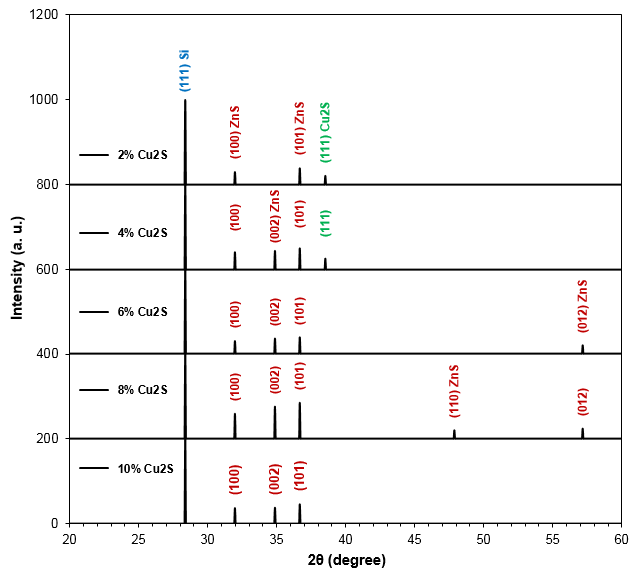
Figure (1) shows the XRD patterns of Cu2S-doped ZnS films deposited on Si(111) substrates at different doping ratios (2, 4, 6, 8 and 10 at.%). It can be observed from these patterns that the peaks (31.9403, 34.5121, 36.3949, 47.6923 and 57.0149) refer to (100), (002), (101), (012) and (110) directions, respectively. These patterns coincide with those of the hexagonal structure of ZnS. It can be observed that the peak of Si located at 28.35° is related to (111) crystal plane. The preferred peak of ZnS films doped by 2-10 wt.% Cu2S ratio appear at 36.39 for (101) plane while the preferred peak of Cu2S is located at 38.40 for (111) crystal plane. It can be noted that the grain size and dhkl decrease with increasing doping ratio of Cu2S and the maximum value is observed at doping ratio of 10%.

Fig. (1) X-ray diffraction patterns of Cu2S-doped ZnS films deposited at different doping ratios (2, 4, 6, 8 and 10 wt.%)
Figure (2) shows the XRD patterns of porous p-type Si (111) at different etching times. These patterns show the difference between silicon wafer and porous silicon, where the strong peak of pure Si appears at 28.35 along the (111) direction confirming the monocrystalline structure of the Si layer belonging to the (111) plane of Si cubic structure. Increasing etching time results in broadening of the peak with varying full-width at half maximum (FWHM), as shown in Fig. (2). The thickness of the porous structure is decreasing with increasing etching time and the reduction in the crystallite size can be inferred through the increase in broadening of the XRD spectra.

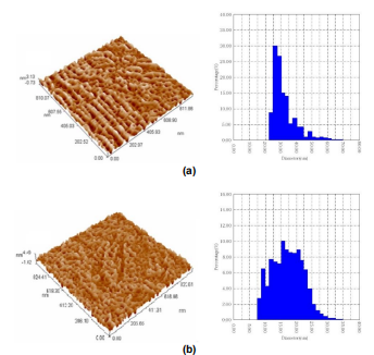
Fig. (3) AFM images of porous Si wafer prepared at constant current of 40 mA and etching times of 10min (a) and 50min (b)
4. Conclusions
Polycrystalline Cu2S-doped ZnS structures were successfully prepared as thin films by PLD method. These structures were deposited on the surfaces of porous silicon samples prepared by electrochemical etching method. The topography of porous silicon shows a decrease in average diameter with increasing etching time. The photoluminescence emission spectrum has a broad blue range with increasing porosity time.
上一篇: 减少150mm硅衬底污染的方法
下一篇: 掺杂硅的室温电学特性