ABSTRACT
Hyperdoped silicon is a promising material for near-infrared light detection, but to date, the device efficiency has been limited. To optimize photodetectors based on this material that operate at room temperature, we present a detailed study on the electrical nature of gold-hyperdoped silicon formed via ion implantation and pulsed-laser melting (PLM). After PLM processing, oxygen-rich and gold-rich surface layers were identified and a wet etch process was developed to remove them. Resistivity and Hall effect measurements were performed at various stages of device processing. The underlying gold-hyperdoped silicon was found to be semi-insulating, regardless of whether the surface gold was removed by etching or not. We propose a Fermi level pinning model to describe the band bending of the transformed surface layer and propose a promising device architecture for efficient Au-hyperdoped Si photodetectors.
I. INTRODUCTION
Hyperdoped semiconductors contain an intermediate band (IB, a.k.a. impurity band) within the bandgap that can be employed to efficiently absorb light with below bandgap energies and are promising candidates for Si-based near-infrared (NIR) photodetectors.These materials are typically fabricated by ion implantation of a suitable impurity followed by pulsed laser melting (PLM) to achieve the high impurity concentrations required to form an IB (6x1019 cm-3for Si ).
Among the various transition metal impurities explored to date, gold (Au) is the only impurity that can be homogeneously hyperdoped in mono-crystalline Si up to concentrations of 1020 cm -3, above which filamentary breakdown takes place.Other impurities tend to segregate completely or exhibit filamentary breakdown.Despite showing broadband NIR optical absorption and photoresponse, Au-hyperdoped Si detectors have an extremely low quantum efficiency (, 0:01%),which has been attributed to poor carrier transport and carrier lifetime properties within the hyperdoped layer (10–800 ps).We have recently suggested that the NIR light detection efficiency in Au-hyperdoped Si devices at room temperature (RT) can be improved with an optimized device architecture.To achieve this, accurate knowledge of the surface properties and RT electrical characteristics of the Au-hyperdoped layer is required.
In terms of the surface properties, it is well known that some degree of Au surface segregation will occur during the PLM process due to the high interface diffusivity of Au and the low solid solubility of Au in the solid phase of Si as compared to its liquid phase.This phenomenon is well evidenced by Rutherford backscattering spectrometry and ion channeling (RBS-C) and secondary ion mass spectrometry measurements.It is also expected that the Si surface may become oxidized during the PLM process. This will greatly impact the quality of metallic contacts formed directly on the Au-hyperdoped Si. In turn, this can complicate interpretation of near-surface electrical measurements.
Here, we investigate the impact of the surface on the measured electrical characteristics of Au-hyperdoped Si formed by ion implantation and PLM. We first focus on the physical surface properties of Au-hyperdoped Si. Wet etching experiments are combined with RBS-C measurements to gain a better understanding of the Au-hyperdoped Si surface. Van der Pauw resistivity and Hall measurements are then reported. Finally, we discuss the origin of the so-called anomalous n-to-p type-conversion phenomenon described above.
II. EXPERIMENTAL METHOD
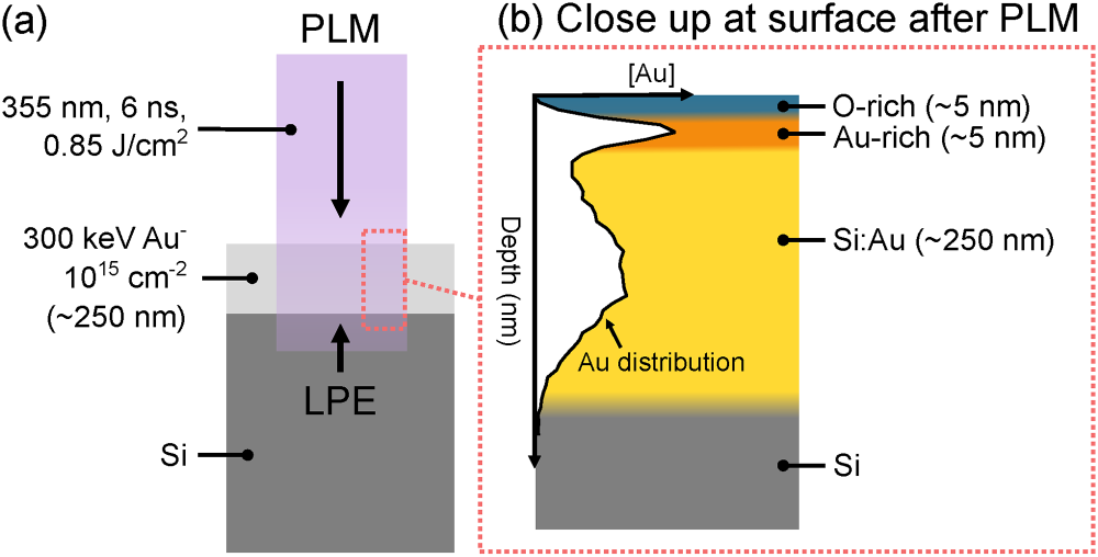
Au-hyperdoped Si samples were fabricated by ion implantation and PLM as described in our previous works.Briefly, Auþ ions at 300 keV were implanted into a semi-insulating float-zone Si substrate (sourced from Topsil Global Wafers, ρ . 10 kΩ cm, h100i, 310–340 μm thick) held at 77 K at an ion fluence of 1015 cm-2. The high resistivity ensures that a doped surface remains electrically isolated from the substrate. Indeed, this behavior has been confirmed with implanted Bi on similar substrates.20 During implantation, the Si substrate was tilted by 15。 and rotated by 7。to minimize ion channeling. PLM was then performed with a single 6 ns pulse of the third harmonic (355 nm) of a Nd:YAG laser (Ekspla) over a 2.5x2.5 mm2 aperture to a nominal fluence of 0.85 + 0.05 J/cm2. A schematic of the PLM process and sample cross section after PLM together with the resultant Au concentration profile is shown in Fig. 1. The melt duration was monitored using time-resolved reflectivity with a 488 nm Arþ ion laser. The PLM was tiled in a 2x2 configuration with a slight overlap to create a single Au-hyperdoped Si sample with an area just under 5x5 mm2. The sample was then diced along the perimeter of the PLM region into a 4 x4 mm2 chip with an Oxford Lasers ALPHA 532-XYZ-A-A Laser Micromachining Tool to electrically isolate it from the surrounding amorphous Au-implanted region. All samples were then subjected to sonication in acetone, IPA, and DI-H2O, followed by various wet etch procedures described in Sec. III A.

FIG. 1. (a) Schematic of the PLM process. Rapid solidification and liquid phase epitaxy (LPE) occurs within hundreds of nanoseconds following the laser pulse. (b) Sample cross section after PLM, showing the O-rich layer at the surface (blue), the Au-rich layer (orange) underneath due to Au surface segregation from PLM, and the underlying Au-hyperdoped layer (yellow). The Au concentration [Au] distribution is shown as a black trace shaded white (data are the same as that shown in Fig. 2 labeled “as-PLM”).
III. RESULTS AND DISCUSSION
A. Surface etching experiments
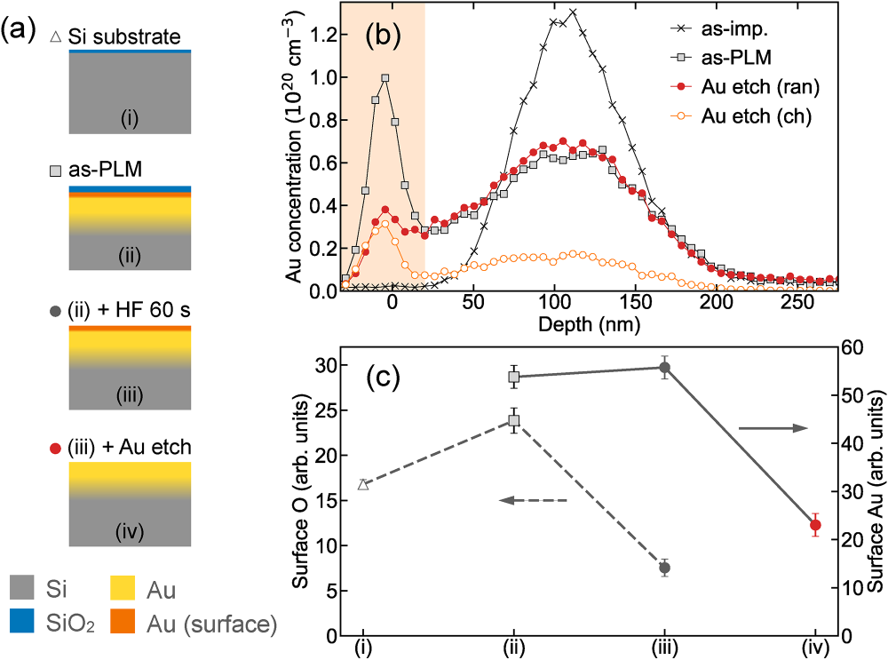
To electrically contact the Au-hyperdoped Si effectively, a series of wet chemical processes were investigated. Figure 2(a) schematically shows the samples after each processing step. A Si substrate with a native surface oxide [Fig. 2(a)(i)] was implanted with Au and PLM processed [Fig. 2(a)(ii)] as described above. Afterward the sample was cleaned in Piranha (10 min in H2SO4: H2O2 ¼ 4 : 1 at 90℃ HCl:HC), dilute HF (5%, 10 s), and RCA2 (10 min in 2O2:H2O = 1:1:5 at 90℃). A longer HF etch was performed for 60 s [Fig. 2(a)(iii)]. This was followed by a Au etch process, which involves repeatedly etching (three times) in HF for 45–60 s followed by an 8 min aqua regia etch (3:1 of HCl and HNO3) [Fig. 2(a)(iv)].

Fig2
Figure 2(c) shows the integrated O and Au concentrations at the Si surface determined by RBS. It is observed that the PLM process results in an increase in the surface oxide thickness [denoted as a blue layer in Fig. 2(a)(ii)]. This is consistent with our previous reports in Ag-hyperdoped Si.8 Other than the high temperatures experienced by the Si during PLM in atmosphere, oxidation may also result from Au and Ag acting as oxidation catalysts in Si.A HF etch of 60 s is shown to remove this oxide. We find that at least 45 s of HF etching is required for its removal and greater than 60 s did not appear to reduce the O content any further. The small persisting O signal is presumably due to near surface O beneath the surface and/or oxide regrowth during sample transport between the HF lab and the RBS sample chamber.
B. Electrical measurements
Three van der Pauw samples were prepared for resistivity and Hall effect measurements, including an intrinsic Si sample [substrate control, Fig. 2(a)(i)], Au-hyperdoped Si sample after 60 s etching in dilute HF [HF 60 s, Fig. 2(a)(iii)], and Au-hyperdoped Si sample after the Au etch procedure [Au etch, Fig. 2(a)(iv)]. Before the evaporation of the Al electrodes, these samples were further etched in dilute HF to remove the surface oxide (otherwise, the I–V characteristics of our devices become non-linear). In short, after device processing, the surfaces of our three devices consist of either a clean Si surface, Au-hyperdoped Si with a significant Au segregated surface, or Au-hyperdoped Si with a greatly reduced Au segregated surface.
C. Fermi level pinning model
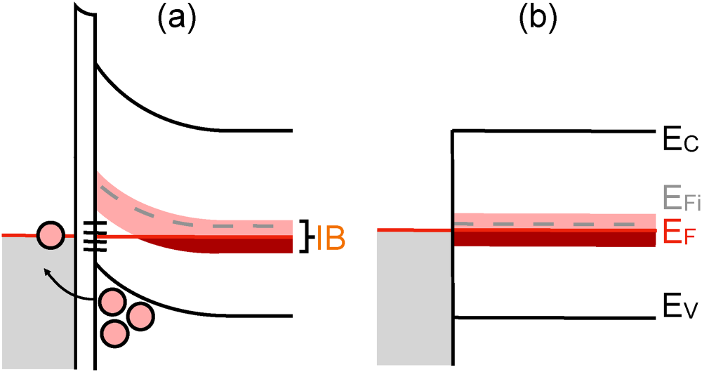
We propose a surface Fermi level pinning model and discuss how it may adequately explain the aforementioned n-to-p-type conversion phenomena in Au-hyperdoped Si at RT. The surface band diagram of our Fermi level pinning model is shown in Fig. 3(a). From theory, the Au-hyperdoped layer, which has a peak Au concentration in the bulk of 7x1019 cm-3 in our work [Fig. 2(b)], should result in the formation of a partially filled IB in the Si bandgap located between the two Au deep donor and acceptor energy levels. At RT and under the dark measurement conditions employed, we do not expect the IB to be ionized and thus, the Fermi level will appear within the IB. Note that even though this Fermi level model agrees well with our observation that Au-hyperdoped Si is semi-insulating, we acknowledge that this observation alone does not constitute evidence for the formation of a partially filled Au-IB nor the location of the Fermi level, as will be discussed later.
From Fig. 3(a), it is clear that Fermi level pinning causes the surface bands to bend in the same way as if the surface was heavily doped with shallow p-type dopants. This enables the formation of Ohmic contacts to the semi-insulating Au-hyperdoped Si, as suggested by our Hall effect measurements.Furthermore, under our Fermi level pinning model, it is expected that Au-hyperdoped Si will be rectifying on n-type Si substrates and Ohmic on p-type substrates, as observed in the literature.In light of recent reports on Ti-hyperdoped Si in the literature,it may be beneficial to perform further measurements on Au-hyperdoped Si at low temperatures to achieve electrical isolation from the substrate and to confirm the formation of a Au-IB. Additionally, x-ray techniques may also be employed to elucidate the location of the Fermi level and provide further evidence that supports the existing theory.

FIG. 3. Proposed band diagram under equilibrium conditions (zero bias) of (a) Au-hyperdoped Si with an interface layer of atomic dimensions (a few Å, either from a mildly oxidized surface or a vacuum layer) and segregated Au sandwiched between it and the metal contact (Al); (b) Au-hyperdoped Si directly in contact with metal, assuming perfectly ideal conditions with no surface states or band bending. Pink dots represent hole carriers, gray area represents electrons in the Al metal, pink (dark red) area represents empty (filled) states in the Au-IB, acceptor states due to interaction between Au and surface/interface states are represented by black solid lines. The red solid line represents the Fermi level (EF) while the intrinsic Fermi level in Si (EFi ) is represented by dashed gray lines. The VB/CB edge is indicated by EV/EC.
IV. CONCLUSION
To summarize, the extensive use of the RBS-C technique has provided us with a better understanding of the surface properties of Au-hyperdoped Si and has enabled us to develop a reliable wet etching protocol that removes the enhanced surface oxide and reduces the amount of surface segregated Au. This allowed us to gain a better understanding of the electrical characteristics of the Au-hyperdoped Si at RT and investigate the effect of the Au surface segregation. Hall effect measurements indicate that our Au-hyperdoped Si samples are semi-insulating at RT, in agreement with theoretical predictions. Furthermore, previous experimental observations of p-type conduction in Au-hyperdoped Si may be a result of Fermi level pinning at the surface and subsequent band bending, and/or measurement of the substrate. Additional X-ray measurements and low temperature photoconductivity measurements may provide a more robust confirmation of theoretical predictions about the formation of a Au-IB in our samples, the location of the Fermi level, and whether Au-hyperdoped silicon will lead to useful applications in optoelectronics. Our work provides insight into the surface properties of Au-hyperdoped Si and proposes a method to fabricate Au-hyperdoped Si photodetectors that operate at RT with improved reliability and efficiency.