Abstract— High-temperature operation of the p-GaN gate high-electron-mobility transistor (HEMT) was investigated, specifically up to 500℃. The p-GaN gate HEMT demonstrated stable behavior with normally-off operation, steep increase of drain current in the subthreshold region, and suppressed off-state current. By adding Al2O3 etch-stop layer, the device showed significant reduction in subthreshold swing when measured at 500℃, effectively mitigating hysteresis in the transfer characteristics. Additionally, the lifetime of the gate stack with the etch-stop layer was estimated to be much longer than that of the stack without the etch-stop layer. Through the integration of the depletion-mode (D-mode) metal-insulator-semiconductor HEMT (MIS-HEMT) device with the p-GaN gate device, a direct-coupled field-effect transistor logic (DCFL) inverter was fabricated. This inverter showed stable logic operation up to 500℃, featuring rail-to-rail operation and large gain. A long-term reliability test conducted at 500℃ for 100 hours revealed stabilized on-state and off-state values after about 50 hours of operation.
I. INTRODUCTION
HIGH temperature electronics have gained significant attention across industries, including aerospace, automotive, and energy production. Challenges faced by conventional electronics under high temperature conditions, such as increased leakage current and poor stability, have prompted extensive research into wide bandgap materials. Among these materials, GaN has demonstrated significant promise due to many advantages, including large bandgap, high breakdown field, excellent thermal stability, and high saturation velocity.
In this study, we demonstrated stable high temperature operation of the p-GaN gate HEMT up to 500℃. By incorporating etch-stop layer, the p-GaN interface was effectively protected from dry etching induced damage, resulting in longer gate stack lifetime and reduced hysteresis. The device showed stable normally-off operation for 100 hours without significant degradation or breakdown at 500℃. Furthermore, we tested the operation of DCFL inverter utilizing the p-GaN gate HEMT up to 500℃, demonstrating the feasibility of high temperature logic operation.
II. DEVICE FABRICATION
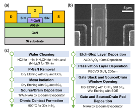
The p-GaN gate HEMT device was fabricated on the pGaN/AlGaN/GaN heterostructure grown on silicon substrate. The substrate consists of 70 nm p-GaN, 15 nm Al0.2Ga0.8N, 0.7 nm AlN, 200 nm unintentionally doped GaN, 5.8 µm GaN buffer, and silicon substrate from top to bottom. The schematic of the device is shown in Fig. 1(a), and the top-view scanning electron microscopy (SEM) image of the fabricated device is shown in Fig. 1(b). The length of gate electrode/p-GaN contact area was 1.5 µm, and the width was designed to be slightly smaller than the width of the mesa-isolated AlGaN/GaN block to prevent the electrodes from directly contacting the sidewall, which may have dry etching induced damage. The fabrication process is shown in Fig. 1(c). The p-GaN layer on top of the substrate was removed, and mesa isolation was carried out by dry etching performed using inductively coupled plasma reactive ion etching (ICP-RIE) with Cl2 and BCl3. Ti/Al/Ni/Au (20 nm/120 nm/60 nm/ 50 nm) stack was then deposited as the source/drain electrode using e-beam evaporator, followed by rapid thermal annealing at 900 ◦C for 30 seconds in N2 to form the ohmic contact. 10 nm of Al2O3 etch-stop layer was deposited using atomic layer deposition (ALD), and 200 nm of Si3N4 layer was deposited using plasma-enhanced chemical vapor deposition (PECVD). Gate stack and source/drain contact windows were opened by ICP-RIE using SF6, and the ALD Al2O3 etch-stop layer was removed by wet etching using buffered oxide etch (BOE). Ni/Au (50 nm/150 nm) layer was deposited as the gate electrode using the e-beam evaporator, and post-metallization annealing was performed at 500 ◦C for 5 minutes in N2.

Fig1
III. RESULTS AND DISCUSSION
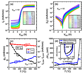
Temperature dependence of the transfer characteristic and gate leakage current of p-GaN gate HEMT with etch-stop layer are shown in Fig. 2(a) and 2(b), respectively. For the high temperature measurements, the device was measured in vacuum environment, with contact made using probe tips. The gate voltage was increased and decreased in steps of 0.1 V, with time interval of approximately 0.2 seconds between each gate voltage value, and there was no delay introduced between the forward and backward sweeps. The device showed stable high temperature operation with suppressed off-state current and sharp subthreshold slope. Normally-off operation was maintained with slight threshold voltage shift towards the negative direction, from 1.4 V at 25℃ to 0.9 V at 500℃, estimated by the gate bias at which the drain current is 10−2 mA/mm. The gate leakage current gradually increased with increasing temperature, but the gate stack demonstrated stable operation without breakdown, even with large gate bias of 8 V up to 500℃. Fig. 2(c) shows temperature dependence of the on-state current, off-state current, and peak transconductance. As the temperature increases, the on-state current gradually decreased, off-state current gradually increased, and the transconductance decreased. As the temperature increases, the mobility of the channel formed at the AlGaN/GaN interface decreases primarily due to increased phonon scattering, leading to a decrease in the on-state current and transconductance. The off-state drain current can be attributed to the carrier hopping current flowing through the dry etching induced traps on the AlGaN and GaN surfaces, which can be further suppressed by optimizing the dry etching recipe.
To investigate the effect of etch-stop layer, another batch of devices without the etch-stop layer was fabricated by depositing PECVD Si3N4 layer directly on the p-GaN layer and then etching it away by SF6 ICP-RIE. The subthreshold swing measured at 500℃ and VTH hysteresis of the transfer curve are shown in Fig. 2(d). The VTH hysteresis (1 VTH) was extracted using the equation 1 VTH = VTH−F – VTH−B, where VTH−F is the threshold voltage in the forward sweep and VTH−B is the threshold voltage in the backward sweep. The device with etch-stop layer had more suppressed hysteresis, especially starting from 475℃. The minimum subthreshold swing of the device with and without the etch-stop layer measured at 500℃ were 283 mV/dec and 619 mV/dec, respectively, indicating sharper increase of the drain current in the subthreshold region with the etch-stop layer. Since the ALD Al2O3 layer showed extremely low etch rate with SF6 dry etching and could be easily removed using BOE, addition of this layer effectively prevented dry etching induced damage on the p-GaN layer. We believe that the reduction of hysteresis and subthreshold swing is attributed to the incorporation of etch-stop layer. Hole injection through the gate metal/pGaN Schottky junction was suppressed by maintaining intact interface with fewer traps, especially at high temperatures and with large gate bias, which led to smaller hysteresis. Furthermore, gate controllability over the channel was enhanced by improving the uniformity of p-GaN layer under the gate, resulting in reduced subthreshold swing.

Fig2
Lifetime of the device was estimated by applying the gate bias on the array of devices with LGS = LGD = 4 µm while source/drain electrodes were grounded. Weibull plots of the time to breakdown (tBD) distribution and lifetime predictions for the devices are shown in Fig. 3(a) and 3(b), indicating lifetime of 10 years for the device without the etch-stop layer at VGS = 4.3 V, and lifetime of 10 years for the device with the etch-stop layer at VGS = 5.9 V. Therefore, the addition of the etch-stop layer, which serves to protect the p-GaN surface, significantly improves the lifetime of the gate stack, highlighting the importance of preserving the intact p-GaN interface.

Fig3
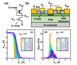
High temperature operation of the DCFL inverter was thoroughly tested. The circuit diagram and schematic of the DCFL inverter are illustrated in Fig. 4(a) and 4(b), respectively. The enhancement-mode (E-mode) p-GaN gate HEMT device and D-mode MIS-HEMT device were integrated with channel width ratio of 100:1. For the D-mode device, the p-GaN layer was completely removed, and 20 nm ALD Al2O3 layer was used as the gate oxide. Temperature dependent transfer characteristics and gain of the DCFL inverter are shown in Fig. 4(c) and 4(d), respectively. The transfer curve showed stable operation up to 500 ℃, maintaining sharp transition region and consistent rail-to-rail operation with output voltage range from approximately 0 V to 5 V. This inverter demonstrated high gain that gradually decreased as the temperature increased, ranging from peak gain of 30.8 V/V at 25℃ to 9.1 V/V at 500℃.

Fig4
IV. CONCLUSION
In summary, the p-GaN gate HEMT with the etch-stop layer demonstrated stable operation up to 500℃, and long-term reliability was further confirmed by the consistent performance observed during 100 hours of device characterization at this temperature. By utilizing the etch-stop layer to preserve the intact p-GaN surface and avoiding direct contact of the gate electrode on the mesa sidewall, the device showed suppressed off-state current, steep subthreshold slope, and improved hysteresis. Additionally, long-term reliability test confirmed reasonably long device lifetime with appropriate supply voltage, and stable high temperature operation of the DCFL inverter was also examined. We believe that this p-GaN gate device with the etch-stop layer is a strong candidate for high temperature logic device, opening another path for development of high temperature electronics.
上一篇: 掺杂硅的室温电学特性
下一篇: 用于集成光子学的 GaN_AlN 双层