Abstract: III-Nitride semiconductors offer a versatile platform for integrated photonic circuits operating from the ultra-violet to the near-infrared spectral range. Either pure AlN or pure GaN waveguiding layers have usually been investigated so far. In this work, we report on the study of GaN/AlN bilayers epitaxially-grown on a sapphire substrate for photonic circuits. Quality factors up to 410,000 are demonstrated with microring resonators in the near-infrared spectral range. We emphasize the peculiar advantages of these bilayers for nonlinear photonics: GaN offers a larger nonlinear susceptibility as compared to AlN. More importantly, both materials exhibit nonlinear susceptibilities with opposite signs that can be advantageous for nonlinear conversion. Thick epitaxial III-nitride bilayers are associated with the occurrence of cracks in the epi-layers and multimode waveguide propagation. We show that the multimode character can lead to peculiar resonance line shapes with the capacity to control full transmission and reflection by phase engineering.
1. Introduction
Several platforms have been investigated to develop photonic circuits operating in the Ultra-Violet or in the visible spectral range. Among many examples, one can cite platforms based on silicon nitride, silicon carbide, diamond, lithium niobate. As wide band gap semiconductors, the III-nitrides like gallium nitride (GaN) and aluminum nitride (AlN) present specific advantages as they can provide all functionalities needed for an universal platform (waveguides, resonators, detectors, lasers, modulators, phase shifters, couplers with grating or tapers, directional couplers, beam-splitters etc). One specific advantage of III-nitrides as direct band gap semiconductors is their capacity for monolithic integration of laser sources, a feature not directly available with silicon nitride, silicon carbide, diamond or lithium niobate. As the crystalline structure of III-nitrides is non-centrosymmetric, the III-nitrides give access to second-order nonlinear processes, including second harmonic generation, spontaneous downconversion and electro-optic effect. The III-nitride semiconductors can be epitaxially grown on sapphire and on Si(111) substrates with large wafer sizes up to 300 mm, thus offering opportunities for integration and compatibility with silicon fabrication environment.
In the literature, most studies are dedicated to thin films made of AlN or thin films mostly made of GaN, albeit a thin AlN layer to ensure proper nucleation. High quality factor resonators have been demonstrated using both types of materials in microring resonators, with intrinsic quality factors above one million in the near-infrared spectral ranges. Values in the same range have also been demonstrated at shorter wavelengths (390 nm) in a spectral domain where the losses are dominated by scattering. These results, among others, highlight the maturity of the III-nitride platform for photonics.
Combining GaN and AlN in forms of bilayers offer specific advantages. GaN has a larger second-order nonlinear susceptibility as compared to AlN with absolute values reported in the literature ranging from 10 to 23 pm/V for GaN while values ranging from 4 to 8 pm/V have been reported to AlN. This is a consequence of a closer band edge proximity for GaN as compared to AlN. Benefiting from a larger nonlinear susceptibility is a plus as conversion efficiencies scale with the squared value of this parameter. Furthermore, GaN and AlN exhibit opposite signs of their nonlinear susceptibility. This feature is quite unique as compared to other platforms as one can epitaxially engineer bilayers that provide an enhanced conversion efficiency for nonlinear processes. This intrinsic polarity inversion is easier to handle by epitaxy as compared to other techniques such as wafer bonding or patterning and domain regrowth which can lead to polarity inverted structures but result in increased losses.
2. Sample fabrication
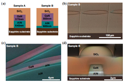
The III-nitrides were grown on sapphire substrate by metalorganic vapor phase epitaxy (MOVPE) in a showerhead 7x2 in. reactor with an AlN layer followed by a GaN layer. The growth was performed using H2 carrier gas. Trimethylgallium, trimethylaluminum (TMAl) and ammonia were used as precursors for Ga, Al and N, respectively. Two types of samples were investigated: a 640 nm thick AlN layer followed by a 570 nm thick GaN layer (sample A) or a 600 nm thick AlN layer followed by a 800 nm thick GaN layer (sample B). The growth proceeds through several phases. The interface layer between the sapphire substrate and the AlN layer plays a critical role. The sapphire substrate is annealed at 1080◦C under H2 for 10 min at a pressure of 100 mbar. The surface is then exposed at a temperature of 940◦C to a 14 standard centimeter cube per minute (sccm) flow of TMAl for 7 s. A 3 monolayer-thick AlN buffer layer is then grown for 20 s with a TMAl flow of 14 sccm and an ammonia flow of 160 sccm. The pressure is then decreased down to 25 mbar and the temperature increased to 1140◦C for the growth of a 600 nm-thick layer at a 13 nm/min growth rate. Two identical AlN templates were grown in the same run, following the provided procedure. These templates were loaded separately for the growth of the rest of the structure. For sample A, an additional 40 nm-thick AlN layer was grown at 1140◦C followed by a 570 nm-thick GaN layer at 1060◦C. For sample B, a 800 nm thick GaN layer is grown at 1040◦C. Figure 1(a) shows a schematic of the epitaxial layers.

Fig1
The GaN growth on the AlN template layer initially exhibits an initial 3-dimensional growthmode followed by a progressive smoothing of the GaN layers. A GaN thickness larger than 500nm is required to get a fully coalesced GaN layer under our growth conditions. For a 10x10 μm2 atomic force microscopy scan size, the root mean square roughness is 7.9 nm, 2.1 nm and 1 nmwhen the GaN thickness is 290 nm, 550 nm (sample A) and 800 nm (sample B), respectively.illustrating the effective smoothness achieved through coalescence.
3. Optical characterization
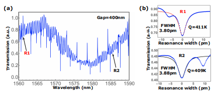
Figure 2(a) shows the near-infrared transmission spectrum of the 600/800 nm thick AlN/GaN bilayer structure (sample B). First, small oscillations with a 0.4 nm periodicity can be observed. They correspond to a Fabry-Perot type feedback from the cleaved facets of the 1.5 mm long waveguide. More importantly, one can observe sharp resonances that are associated with the microring resonances. At 1561 and 1585 nm, a resonance with a loaded quality factor of 410 000 is measured. A zoom on these resonances are shown in Fig. 2(b). This value is obtained with a relatively narrow ring width (1.5 µm) that is more sensitive to sidewall scattering. In the literature, higher quality factor values have been reported with epitaxial layers consisting of either only GaN (2.5 Million) or only AlN (2.5 Million). The present result shows that significantly high quality factors can be achieved with AlN/GaN bilayers even if they are smaller than the record values of single layers. For these structures, we did not obtain better results following high temperature thermal annealing that can decrease the SiO2 residual absorption. The GaN layer cannot be annealed at temperatures as high as AlN thus limiting the added value provided by high-temperature annealing for AlN. One specific advantage of the AlN/GaN bilayer is associated with the fact that the first-order optical mode in the vertical direction like the TM10 or the TE10 mode can have lobes distributed in the AlN and GaN region if the GaN thickness is limited to 300-400 nm. This characteristic allows for an enhanced nonlinear conversion efficiency by using the intrinsic polarity inversion that exists between AlN and GaN, i.e. opposite values of the second-order nonlinear coefficient, as previously discussed in Ref.

Fig2
下一篇: 多晶 Mo 纳米线的受控分步湿法蚀刻