With the persistent downscaling of integrated circuits, molybdenum (Mo) is currently considered a potential replacement for copper (Cu) as a material for metal interconnects. However, fabricating metal nanostructures with critical dimensions of the order of 10 nm and below is challenging. This is because the very high density of grain boundaries (GBs) results in highly non-uniform surface profiles during direct wet etching. Moreover, wet etching of Mo with conventional aqueous solutions is problematic, as products of Mo oxidation have different solubility in water, which leads to increased surface roughness. Here, a process is shown for achieving a stable and uniform soluble surface layer of Mo oxide by wet oxidation with H2O2 dissolved in IPA at −20 °C. The oxide layer is then selectively dissolved, and by repeating the oxidation and dissolution multiple times, a uniform etch profile is demonstrated with a fine control over the metal recess. Ultimately, this presents a method of precise and uniform wet etching for Mo and other metals needed to fabricate complex nanostructures that are critical in developing next-generation electronic devices.
1. Introduction
The ever-growing demand for high-performance and powerefficient microelectronic devices has driven the semiconductor industry to downscale the transistors and metal interconnects.The interconnects are the nanocrystalline metal nanowires (NWs) connecting the transistors, and copper (Cu) has been used as the core metal of interconnects over the past two decades.However, as the critical dimensions of NWs decrease below 10 nm, the resistivity of Cu becomes much higher than in the bulk due to the long electron mean free path.Thus, there is a strong need for alternative metals, such as molybdenum (Mo), cobalt (Co), and ruthenium (Ru), that outperform Cu at the sub-10 nm scale. Among these metals, Mo is the most promising candidate because, in addition to its lower nanoscale resistivity versus Cu, Mo also allows for a barrier-less process, saving more room for the core metal.
At the nanoscale, the electrical resistivity of metal NWs is strongly affected by the electron scattering from the surface and grain boundaries (GBs).Chemical wet etching is the fabrication step that affects uniformity and surface roughness of metal NWs the most, so it is imperative to achieve a smooth (isotropic), atomic-level controlled, and selective etching process.Nevertheless, controlled and uniform wet etching of nanocrystalline Mo NWs is challenging because of the varying etching rates for different grain orientations and GBs. Hence, understanding and developing reliable wet etching processes for nanocrystalline metals such as Mo is critical for the future fabrication of semiconductor devices. While direct wet etching of single nanocrystals has been extensively studied and fairly well understood,the etching process for nanocrystalline metals is more complex and diffi- cult to control due to the effects of different grain orientations and GBs at the surface.A two-step approach involving selflimiting metal oxidation followed by selective oxide dissolution has been proposed for better etching control.Nonetheless, self-limiting wet oxidation of Mo has not yet been achieved, with only thermal oxidation currently available.

Fig1
Here, we explored the dynamics of wet etching of polycrystalline Mo NWs with hydrogen peroxide (H2O2) solutions. We tracked the direct etching of the Mo NWs with 1% (v/v) H2O2 aqueous solution using in situ liquid phase transmission electron microscopy (LP-TEM) and observed the formation of etching non-uniformities, in particular at the GBs. We show that the etching profile of Mo NWs becomes significantly more uniform when water is substituted with isopropyl alcohol (IPA) as a solvent. Furthermore, we demonstrate the first instance of wet chemical oxidation of Mo for the two-step approach by adjusting the reaction temperature, thus reducing the Mo oxide dissolution rate to a negligible rate. We show that this process can be repeated in multiple cycles for the uniform and controllable recess of the Mo NWs.
2. Results and Discussion
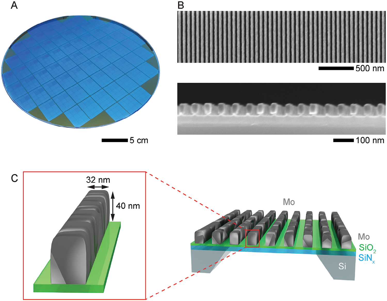
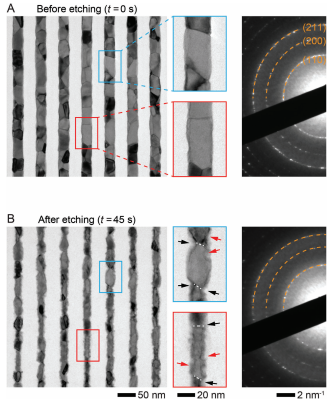
To observe the etching process of a natural nanocrystalline Mo surface, we used wafer-scale patterned Mo NWs similar to the metal lines envisioned to serve as interconnects in future microelectronics components (Figure 1A,B). Each NW has a rectangular cross-section with a width of ≈32 nm and a height of ≈40 nm (Figure 1C). We chose an aqueous hydrogen peroxide (H2O2) solution as a chemical etchant, which is the most commonly used etchant for Mo.Before the etching, Mo NWs were smooth and straight, featuring only a minor waviness (Figure 2A). The selected area electron diffraction (SAED) pattern of the NWs corresponds to pure Mo metal with 〈110〉 texture, and we estimated the average grain size of ≈22 nm from TEM images. Figure 2B shows the same NWs after etching in an aqueous H2O2 solution (1% v/v) for 45 s at room temperature. Compared to their initial state in Figure 2A, the mean NW width decreased from ≈31 to ≈21 nm (corresponding to an etching rate of ≈0.1 nm s−1). However, the NW surfaces are now rough, and individual grains are faceted, which is a clear sign of anisotropic etching. Moreover, we observe multiple pits and grooves at grain surfaces and GBs, which indicate an enhanced etching rate at surface defects. The SAED pattern in Figure 2B shows that no new crystalline phases form during the etching process.

Fig2
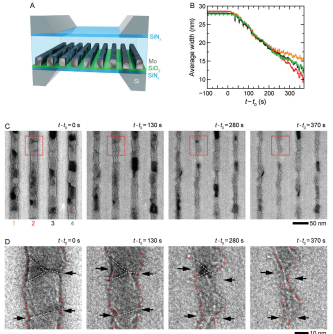
To better understand how the NW surface evolves during the etching, we tracked the entire process in real-time with LP-TEM (Figure 3).The plot of the width of Mo NWs (Figure 3B) extracted from the in situ TEM images series (Figure 3C; Video S1, Supporting Information) shows the gradual width recess for four metal NWs, where the etching rate, defined as the rate of the NW width reduction, remained almost constant at ≈0.02 nm s−1 throughout the etching. However, a closer examination of the selected area in Figure 3D reveals that some pits formed at the GBs at the early stage (Figure 3D: t – t0 = 0–130 s), suggesting that GBs are more susceptible to etching than the sidewalls. As the reaction proceeds, some of these pits also developed faceted edges (Figure 3D: t – t0 = 280–370 s).

Fig3
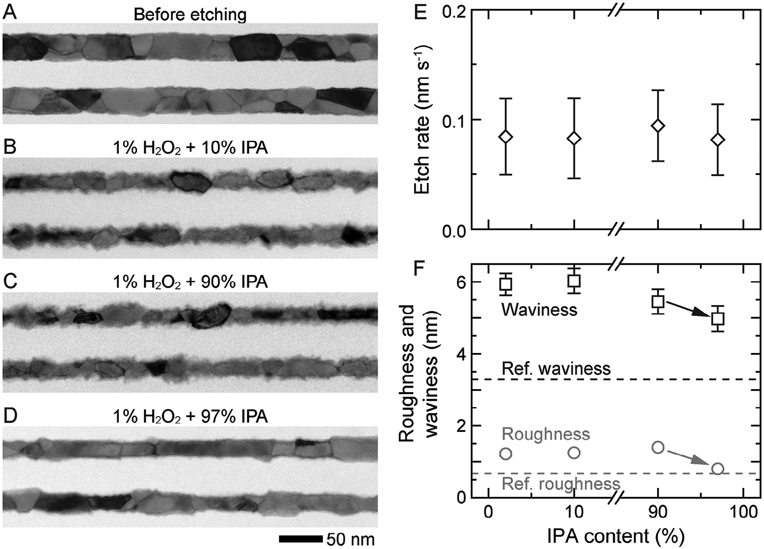
We characterized the surface roughness using a modified line edge roughness (LER) method,separating the small-scale roughness (at the scale of 1–2 nm and below, caused by fastetching in defects and MoO2 masking, below referred to as simply roughness) and the large-scale surface “waviness” (caused by crystallographic anisotropy). Figure 4F compares both surface roughness and waviness after etching with varying IPA concentrations, showing no significant variation of both parameters from 0% to 90% of IPA and a notable reduction of roughness at 97% IPA (as indicated by arrows in Figure 4F). This result con- firms the discussed effect of MoO3 dissolution rate on the etching uniformity.

Fig4
3. Experimental Section
Fabrication of Mo nanowires: First, a 40-nm-thick SiNx film was grown using low-pressure chemical vapor deposition (LPCVD) on both the front and back side of a 300-mm Si substrate wafer (the back side SiNx film serves as a hard mask for patterning the windows and groves for TEM chips, while the front side SiNx layer acts as an electron-transparent membrane). Next, a 10-nm-thick SiO2 layer was deposited on the front side as an etch-stop-layer (ESL), followed by a deposition of 50-nm-thick Mo film on top of the ESL using physical vapor deposition (PVD) at 280 °C. The film was annealed for 20 min at 650 °C in an H2 atmosphere to increase the average grain size of the Mo film. Then, 35-nm-thick of periodic plasmatreated SiNx layer was grown by chemical vapor deposition (CVD) on top of the Mo film as a hard mask, coated first by an amorphous carbon film and then by a metal–organic resist. The resist was patterned using Extreme Ultraviolet (EUV) lithography with periodic 32-nm-wide stripes with a pitch of 64 nm. After SiNx hard mask opening, the Mo NWs were etched using reactive ion etching (RIE) with a Cl2/O2 plasma, stopping on the SiO2 ESL. Dilute HF solution (0.3% v/v) was applied after the RIE process for 15 s for cleaning. After that, SiO2 was filled between the Mo NWs using atomic layer deposition (ALD) at 300 °C to reproduce the actual structure of an interconnect layer. The wafer was then polished using chemical mechanical planarization (CMP), and the SiNx hard mask was selectively removed by RIE. These fabrication steps are summarized in Figure S1 (Supporting Information). Next, individual 5 × 6 mm2 TEM chips were fabricated using optical lithography patterning and RIE. The backside SiNx layer served as a hard mask, and the bulk Si was etched with KOH. Finally, the chips were treated with a dilute HF solution (0.25% v/v) to etch away the SiO2 filling and expose a clean metal surface on the sides of the Mo NWs, as shown in Figure 1B,C. The same chips were used to form the liquid cells shown in Figure 3A. The details of the fabrication steps of the chips and liquid cells are described in our earlier studies.
4. Conclusion
Our direct observations of wet chemical etching of Mo metal NWs in H2O2 reveal that because of varying etch rates along the different crystallographic orientations and associated grain boundaries, direct etching of polycrystalline metals fails to produce uniform etch profiles at the nanoscale. We show that this issue can be overcome by a synergetic approach to manipulating the oxidation product solubility: replacing water with IPA in the etching solution reduces the dissolution rate of MoO3, enabling smooth direct etching, and also allows to decrease the liquid solution temperature to −20 °C to prevent any premature dissolution of the oxide layer that forms on the surface. This enabled us to realize a cyclic “digital” process with solution-based oxidation and dissolution steps, resulting in a great recess control and a highly uniform etching profile with an atomically smooth surface. Importantly, this approach can be readily extended for precise nanoscale wet etching of other metals, and the insights here provide a direct route to enhancing and refining nanofabrication processes in the development of advanced electronic devices.
上一篇: 用于集成光子学的 GaN_AlN 双层
下一篇: 集成光电子器件的进展、前景与挑战