Recently, the emerging 2D materials MXene have gained a surge of attention to the production of optoelectronics devices such as solar cells, plasmonic, phototransistors, photodetectors, light-emitting diodes, photothermal therapy, and so on. Its outstanding optical and electrical characteristics, unique structure, and large specific surface area make it suitable for future use in modern optoelectronics including ultrafast lasers, light emitters, modulators, and plasmonic generators. There is a lack of critical analysis on the prospects, challenges, overview of synthesis methods, mechanisms, and future research directions of MXene despite having some reviews have been published on the applications of MXene. Therefore, this study critically analyzed the existing challenges of MXene, such as poor stability in an oxygen environment, inadequate mechanical properties, ease of stacking, temperature barrier, and so on. In addition, the fundamentals, preparation techniques, properties, and applications of MXene have been summarized. The mechanism, limitations, and benefits of different preparation methods have been mentioned. A comprehensive analysis and guidelines have been provided to improve the existing synthesis methods. The ways to overcome these challenges, prospects, and future markets of the MXene-based optoelectronic devices have been described.
1. Introduction
Over the last decade, optoelectronic devices like solar cells,phototransistors, photodetectors,light emitting diodes,photothermal therapy,[ and so on have improved rapidly in terms of efficiency and quality.Research on optoelectronic devices is at the top of the research ladder for modern optoelectronics and microelectronics. Researchers in this field focus on different outstanding 2D materials such as graphene, MXene, hexagonal boron nitride, black phosphorus, and others.MXene’s superior mechanical strength, electrical conductivity, and surface functionality have made it an essential part of the production of cutting-edge optoelectronic devices. These exceptional properties lead to MXene use in energy storage electrodes,supercapacitors and batteries, enabling optoelectronic applications. The outcome published in the optoelectronics device-related literature indicates high light absorption and photodetection potential, enabling integrated systems. MXene-based photodetectors with improved sensitivity and reaction times revealed their promise for imaging, sensing, and communication systems.Recent achievements have broadened applications of MXene in multifunctional areas including photothermal therapy, lasers, and light-emitting devices in in integrated optoelectronics.
The synthesis of MXene is primarily divided into two types namely top-down and bottom-up methods.The top-down method involves exfoliating bulk crystal volumes into the mono MXene layers, while the bottom-up strategy is considered to be a molecule and atom progress. Top-down techniques have disadvantages such as small crystals, thickness irregularities, and defects in MXene. On the other hand, bottom-up techniques have better crystallinity, fewer defects, and no -F terminations on the exterior. The type of precursor, the synthesis conditions and temperature, the morphology of MXene, and the surface properties, all differ significantly.In the context of the advancement of modern optoelectronics, promising research is being conducted. Heo et al. reported the development of an MXene surface-coated effective solar cell and claimed that its efficiency is 19.69%. However, the improvement of product design and the reduced price of the product should be taken into account.Koo et al.reported that the performance of polyimide-integrated graphene-based electrodes in flexible organic solar cells exceeds 15%. Promising works have been carried out in the preparation of LED. High-performance deep-ultraviolet light-emitting diodes (LED) fabricated on glass with uniform hexagonal boron nitride have been reported.In addition, Ahn et al. published an article in which they used titanium carbide MXene for the development of a highly effective LED. They also introduced a chemical neutral technique to resist the oxidation problem of MXene. Meanwhile, it would be better if they had more elaborate characterization portions.
2. Fundamentals of MXene
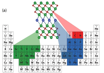
As a result of its layered structure, MXene without delamination looks quite similar to exfoliated graphite. Higher spin-orbital coupling and various spin and oxidation states contribute to the fascinating mechanical and other features seen in the low-dimensional system, notably MXene’s containing transition metals with open D-orbitals. When the aforementioned arrangements of functional groups are optimized for stability, the MXenes are the stable structure that results. For a given structure to remain somewhat stable, it must have many transition metal atoms in its ionic states so that they may donate enough electrons to X and the surface-bound functional groups.The structure of MXene and MAX phase forming elements are illustrated in Figure 1(a–b). In this review article, the properties, synthesis, potential applications, challenges, and scopes will be discussed.

Fig1
3. Properties of MXene
The optical features of 2D materials are of great significance in the fast-growing fields of optoelectronics. The SP2 hybridization of graphene with the honeycomb lattice shape and the extra electron of the Pz orbital leads to linear energy-momentum and increases bonding and antibonding in π-bands in graphene. As a result, they behave as massless Dirac fermions, which leads to a variety of interesting optical and transport phenomena.Dirac electrons have a linearly dispersive nature, which allows them to interact with photon energies over a broad range, thus making them an extremely useful material for a variety of optical and optoelectronics applications.In addition, the layer-based band gap is black phosphorus ranging from 0.3 eV in bulk to 1.5 eV in monolayer structure, making it an outstanding 2D material for application in IR optics,and optoelectronics.
However, MXene has tremendous opportunities and some challenges. The applications including SERS, broadband absorber, and ultrafast laser pulse production have been made possible by MXene. The plasmonic characteristics of Ti3C2TxMXenes, which enable the design of plasmonic devices near IR, have received attention from researchers. In contrast, some challenges were observed, such as gaining a thorough knowledge of MXenes’ optical properties, especially their dielectric characteristics in single- to few-layer MXenes. In addition, poor structural stability and high cost are the key aspects that must be focused on to improve.
4. Preparation techniques of MXene
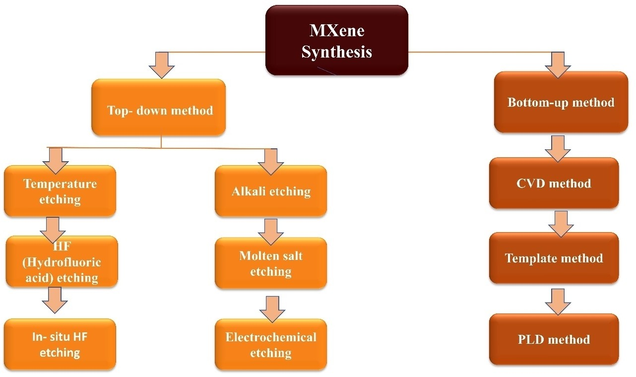
Having been first developed in 2011, MXenes have gained popularity due to the invention of various types of MXenes based on a variety of preparation techniques. Researchers throughout the world are investigating effective ways to overcome MXene’s existing synthesis limitations and developing new synthesis methods that overcome the limitations of previous methods. In the case of HF etching, high concentrations of hydrofluoric acid were required, which are dangerous to humans and the environment. Researchers have continued to strive to find a solution to this limitation and initiate alkali etching, which is environmentally friendly. In such a way, novel types of preparation methods are being developed day by day. The classification of the synthesis of MXene is illustrated in Figure 2. This section covers the most recent research on the types of MXene preparation and a summary of each technique.

Figure 2. Major synthesis process of MXene.
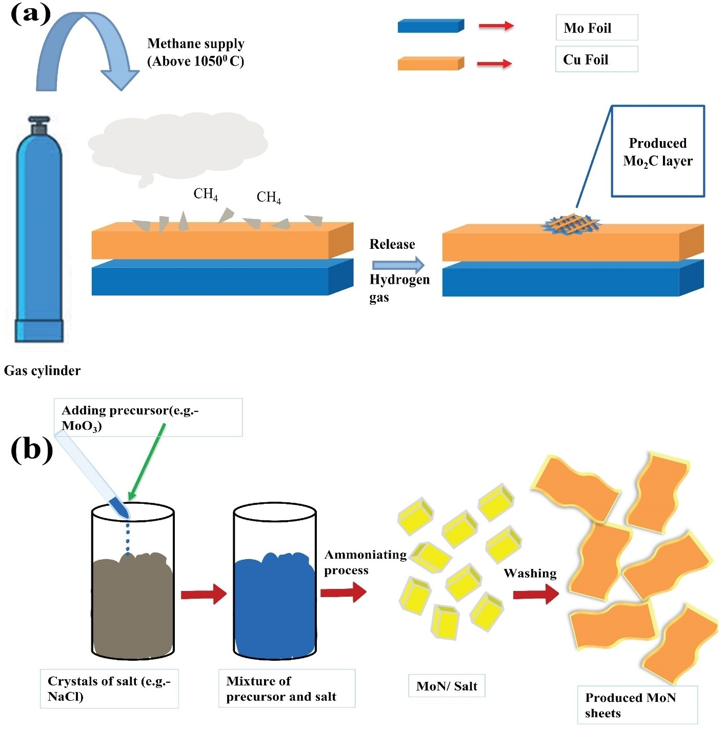
CVD is a method that uses high temperatures and chemicals (Cu, Mo, CH4) in a controlled environment to create MXene, while PLD is used to create a Mo2C layer in Figure 4(a). CVD has higher crystallinity and conductivity, but PLD produces MXene crystals at low temperatures. The synthesis is advancing day by day.

Fig4
5.Conclusions and future outlook
The 2D material MXene has become the most potential for solar cell, plasmonic, and other optoelectronic device materials due to its extraordinary properties. MXene has achieved popularity for different types of MXene based on diverse production processes and a wide range of applications. This study highlights the progress of this substance and its use in the field of optoelectronics. Researchers were able to identify the limitations of MXene and discuss how to overcome them so that they can benefit from it. In addition, the mentioned future research direction including the scope of band gaps and quantum dots for MXene-based modern optoelectronics and digital device production will open a new window for industrialists and scientists. Moreover, limitations have been identified in the work on MXene-based synthesis techniques to meet the global market demand. At present, the global market for MXene is estimated to be worth $26.4 million and is forecast to reach $121.5 million by 2027. MXene, therefore, is in dire need for improvement and must be made commercially feasible for modern optoelectronic devices by overcoming its limitations and enabling it to overcome its limitations. Considering the current and future applications of MXene, as well as addressing existing research challenges and getting a future direction with a solution, this article can be utilized as a credible source and state-of-the-art for researchers.
上一篇: 多晶 Mo 纳米线的受控分步湿法蚀刻
下一篇: III-氮化物发光晶体管的设计