Abstract— This paper describes the design and characteristics of monolithically integrated three-terminal gated III-Nitride light emitting diodes (LEDs) devices. The impact of channel doping and thickness on the voltage penalty of the transistor-LED hybrid device is analyzed, and it is shown that with appropriate design, low voltage drop can be realized across integrated gated LED structures. The impact of device design on the switching charge is investigated, and it is shown that the adoption of an integrated LED/transistor structure can reduce the switching charge necessary for operation of a switched LED display device by an order of magnitude when compared with stand-alone light-emitting diodes.
I. INTRODUCTION
The III-nitride material system has been the key technology enabling solid-state lighting technologies, with widespread applications ranging from the field of general illumination to micro- light-emitting diode (LED) display systems and communications. Emissive display technologies based on GaN/(In,Ga),N heterostructure lightemitting diodes with high pixel density, luminance, efficiency and large color gamut are of great interest for applications such as wearable technologies, mobile devices and virtual displays. While high pixel density requirements for these display applications are fulfilled using scaled (< 15 𝜇𝑚) light-emitting diodes, scaling of the mesa dimensions lead to additional challenges for integration of LEDs and electronic drivers. Besides, it is desirable to have color and luminance variation created using a combination of three colors- red, green, and blue in micro-LED display technologies.
II. THEORY AND DESIGN
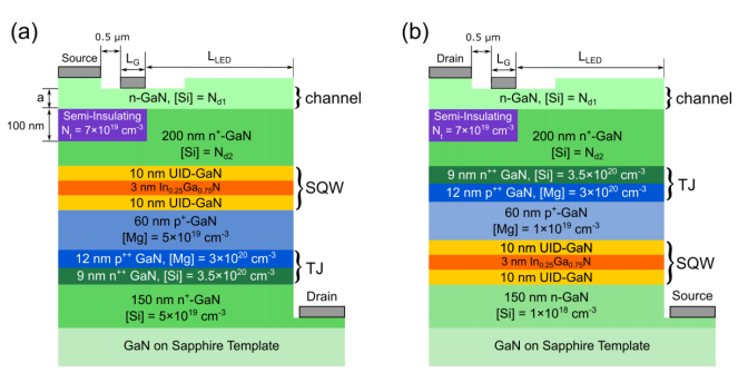
The schematics of the device designs investigated here is shown in Figure 1. It consists of a metal-semiconductor field-effect transistor (MESFET) with GaN/(In, Ga)N based heterostructure LEDs. For the p-down structure, the light emitting transistor (LET) is designed using a bottom tunnel junction-based structure as shown in fig. 1(a), which enables a conductive n-type region on the top surface, which can then be used to create a conductive channel for an nchannel transistor. P-down LEDs (using bottom tunnel junctions) have been reported with low voltage operation and low injection barrier for carriers into the active region. We note that the analysis here is also relevant for both p-up devices with a top tunnel junction as shown in fig. 1(b), with some differences that will be discussed in this manuscript. Recently, experimental demonstration of such an LET was achieved, and is reported separately.

Figure 1. Two-dimensional schematics of the Light Emitting Transistors (LETs): (a) P-down configuration. (b) Pup configuration.
The simulated device consists of a p-down In0.25Ga0.75N QW LED on the top of a GaN homojunction TJ and a lateral depletion-mode MESFET transistor integrated at the top. The fully transparent homojunction TJ design has already been demonstrated to show low voltage drop for LED operation,with a reduced voltage penalty. A green emitting (520 nm) LED above the homojunction TJ was implemented through a 3 nm In0.25Ga0.75N single quantum well (SQW) sandwiched between two undoped GaN barrier layers. No additional AlGaN blocking layer was required in this design for the LED due to a built-in barrier in the InGaN QW that arises from the polarization charges.
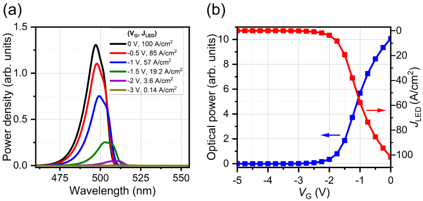
Fig. 4(a) shows the generated optical power spectral density as a function of the wavelength at VDS = 2.9 V which drives a current density of 100 A/cm2 in the on state (VGS = 0). A blue shift is observed in high injection due to quantum-confined Stark effect (QCSE) which is common in InGaN QWs due to the applied electric field. Total optical output power versus gate voltage shown in Fig. 4(b) is extracted by integrating the power spectrum in Fig. 4(a). When switching off the device, the emitted optical power is suppressed by a factor of (~1 × 10⁶ ), which reflects the possibility of a true dimmed device in the off state and high dynamic range.

Figure 4. (a) Simulated emission spectra at VDS = 2.9 V (corresponding to 100 A/cm2 at VGS = 0). (b) Optical output power and gate current versus gate voltage at VDS = 2.9 V.
IV. SUMMARY
To conclude, we designed a monolithically integrated MESFET controlled tunnel-injected 520 nm LED for microLED display systems. The gate of the MESFET designed here controls the electron flow in the LED active region which in turn controls the emission profile of the LED. The design enables high power and efficient voltage modulation of LED with a single epitaxial step. Simulation results show a high on-off current ratio (>105 ) at 100 A/cm2 and (>106 ) at 1 kA/cm2 for high-dynamic-range displays. We also showed that the transistor introduces near zero voltage penalty at 100 A/cm2 indicating a highly efficient operation. The low off current (<1 mA/cm2 ) allows pixels to feature a true black state. The switching charge for an integrated transistor LED proposed here is shown to be significantly lower than a stand-alone LED. We note here that while the 3-terminal device does introduce excess voltage over a standalong LED, it can greatly reduce the complexity of control circuits needed in micro-LED display applications.
上一篇: 集成光电子器件的进展、前景与挑战
下一篇: 微型 LED 的最新进展