Abstract With the advent of technologies such as augmented/virtual reality (AR/VR) that are moving towards displays with high efficiency, small size, and ultrahigh resolution, the development of optoelectronic devices with scales on the order of a few microns or even smaller has attracted considerable interest. In this review article we provide an overview of some of the recent developments of visible micron-scale light emitting diodes (LEDs). The major challenges of higher surface recombination for smaller size devices, the difficulty in attaining longer emission wavelengths, and the complexity of integrating individual, full color devices into a display are discussed, along with techniques developed to address them. We then present recent work on bottom-up nanostructure-based submicron LEDs, highlighting their unique advantages, recent developments, and promising potential. Finally, we present perspectives for future development of micro-LEDs for higher efficiencies, better color output and more efficient integration.
Introduction
III-V semiconductor optoelectronic devices have been widely used in a variety of fields, such as in illumination, displays, data communication, horticulture, and biological detection. To date, however, these applications required individual devices to be relatively large, of the order of a few hundred of microns or more, often driven by the need to maximize the output power1–3 . Now, the development of advanced displays with ultrahigh resolution (e.g., >2,000 pixel per inch (PPI)), especially those for augmented and virtual reality (AR and VR), makes it necessary to use smaller device sizes for improving the resolution4 . Biomedical and visible-light communication applications of microscale light sources have also been of great interest recently4–7 . The micro-LED devices would have the benefits of higher self-emissive brightness, ultra-high integration density, robustness and stability as compared to existing technologies, such as liquid crystal displays (LCDs) and organic light emitting diodes (OLEDs)8 . A comparison of these technologies is shown in Table 1.
The pioneering technology for modern displays was LCDs, using liquid crystals to block emission from a backlight, and colors were attained through color filters. However, it had some limitations including color saturation, slow response times and poor conversion efficiency. More importantly, a large fraction of the optical power generated from the backlight was being wasted in these displays as they were not self-emitting. LCD displays are also difficult to scale down to small sizes with high resolution. Therefore, displays moved towards more energy-efficient self-emitting displays comprised of LEDs, which could be either inorganic (e.g., III-nitride based) or organic LEDs. While OLEDs have been widely adopted in displays, they are not without their limitations. Primary among them is the limited brightness of OLEDs (<1000 cd/m2 ) which is a major drawback. OLEDs also suffer from an efficiency roll-off at higher injection currents, resulting in significantly lower output power than inorganic LEDs. Furthermore, OLEDs need longer burnin times, and they are highly resistive, usually operating at current densities on the order of mA/cm2 from Refs. Moreover, it has remained challenging to achieve high PPI OLED displays due to the shadow effect of the fine metal mask used to define pixels. It has also been difficult to achieve high efficiency OLEDs at shorter emission wavelengths (higher energy photons), severely limiting the performance of blue-emitting devices. Generally speaking, the maximum operational temperature of OLEDs is limited to 50-70 ˚C, and they have much shorter lifetimes than inorganic devices. These issues can be readily solved by using inorganic LEDs, which have excellent stability, robustness, brightness, and long lifetimes. Inorganic LEDs typically reach their peak efficiencies at current densities of ~0.1-100 A/cm2 , making them extremely bright with output luminance greater than 100,000 cd/m2 from Ref. . – a necessity for high-power applications. These features have led to their widespread adoption in diverse applications such as general lighting, automotives, horticulture and medicine.
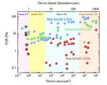
They measured a maximum EQE of ~7% for green microLEDs with device dimensions of 6 × 6 μm37. For devices with red emission, P. Li et al. have examined in detail the temperature dependent properties of red micro-LEDs with an area of 60 μm × 60 μm, and a peak EQE of 3.2% 38. They have also demonstrated a red-emitting micro-LED with a tunnel junction contact, having a maximum EQE of 4.5% . Recently, Y.M. Huang et al. reported a 6 μm × 25 μm sized red micro-LED with a peak EQE of 5.02%, with a focus for visible light communication applications40. A peak EQE of 1.75% has also been demonstrated for a device with 2 μm diameter. The EQE of some III-nitride based LEDs from literature, of different emission colors, are plotted in Fig. 1 for varying device active areas. The EQE of the LEDs shows a drastic reduction when the area of the LEDs becomes smaller for all wavelengths. This reduced efficiency greatly inhibits the commercialization of microLED technology. The causes for this efficiency cliff will be discussed in the next section.

Fig. 1
Regarding the emission wavelength of devices, conventionally, the III-nitrides (AlInGaN) are more generally used for shorter wavelength blue-green emission, whereas the smaller bandgaps of AlInGaP alloys make them better suited for yellow-red emission. However, specifically for micro-LEDs, several factors have motivated the investigation of using InGaN to cover long wavelength red devices as well. Firstly, the bandgaps attainable through the InGaN material system can cover the entire visible spectrum, which could enable full-color redgreen-blue (RGB) devices made from a single material. It has also been shown that InGaN-based LEDs are significantly less impacted by temperature due to the better quantum-confinement of charge carriers, as compared to AlInGaP devices, which improves their usability in applications where heating can affect performance102 . Finally, and most importantly, a lower surface recombination velocity has been measured in the III-nitrides, as compared to AlInGaP, making them a preferable alternative for small-area devices. This is due to the increase in the dominant effect of surface recombination for micro-LEDs especially those with dimensions < 5 μm, which have a high surface-area to volume ratio.
There is a large lattice mismatch between the constituent binary compounds of InGaN alloys – InN and GaN have a lattice mismatch of ~10%. This makes it extremely difficult to grow high-quality InGaN epilayers with emission in the green and red regions of the visible spectrum, due to the tendency of InGaN to form defects and dislocations. The low miscibility of InGaN alloys also causes significant phase separation for high In content alloys, which results in broad luminescence peaks that make it hard to achieve pure red emission. Another consequence of the lattice mismatch is that the grown InGaN epilayers would also be under a large compressive strain, and the resulting strong piezoelectric field spatially separates the electron and hole wavefunctions. The reduced overlap of the carrier wavefunctions limits radiative carrier recombination, further reducing the internal quantum efficiency (IQE). The emission color of the generated light also depends on the injected carrier density. At low carrier injections where the piezoelectric polarization fields cause severe band bending, the emission energy is lower than the bandgap of the alloy. At higher injection currents, where the injected carriers can screen the polarization fields, thereby flattening the bands, the emission wavelength shifts closer to the bandgap. This quantum-confined Stark effect (QCSE) implies a current dependance for the emission color, limiting the applicable brightness range of practical color devices.
Various methods have been developed to enable efficient red emission of InGaN. High-efficiency large-area red and orange LEDs were demonstrated by implementing V-pits to relax compressive strain, thereby helping to increase indium incorporation. The V-pits are usually formed at the start of the growth of the low temperature layer, extending through the active region. They can help enhance the injection of carriers, as holes can be transported from the semi-polar facets of the V-pit into the deeper quantum wells. With the use of this technique, an EQE of 24% was attained for a large-area 1 mm2 LED having emission at 608 nm. However, while the average size and density of V-pits can be somewhat controlled, their location cannot, which is a major detriment to their inclusion in small-area micro-LEDs, where individual devices may randomly contain a few of them.
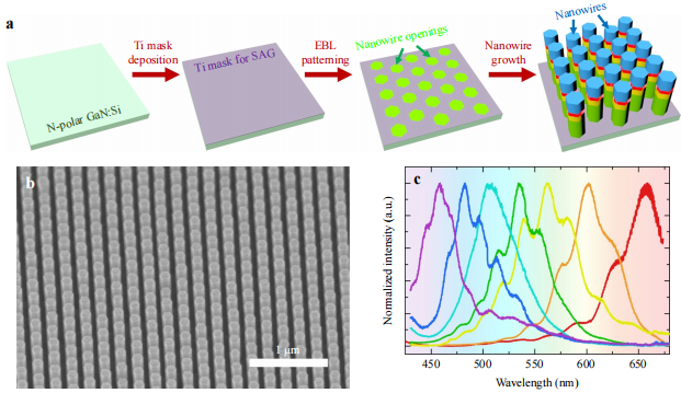
A schematic of the SAE process used in plasma-assisted molecular beam epitaxy is shown in Fig. 2a. Through this process, highly uniform arrays can be grown over relatively large areas, shown in Fig. 2b. The composition of the alloys can be readily tuned by adjusting the ratio of the metal fluxes for the constituent elements (In and Ga). Photoluminescence spectra from nanostructures grown using this method are shown in Fig. 2c, with emission covering the entire visible spectrum. As the incorporation of In depends strongly on the arrangement of nanostructures, due to effects such as adatom migration and flux shadowing from adjacent structures, through this method multiple different InGaN emission colors can be attained.

Fig. 2
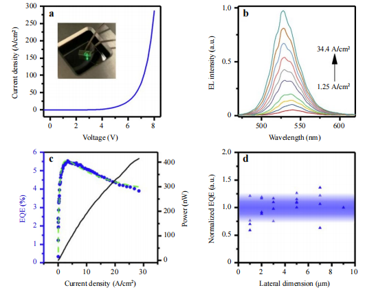
To fabricate the nanowires into micro-LEDs, nanowire arrays were first filled with Al2O3 deposited by ALD, which was then etched back to reveal the top of the nanowires. Plasma-enhanced chemical vapor deposition (PECVD) was then used for depositing a thick SiO2 insulation layer. Stepper lithography was used to etch injection vias into the SiO2 layer to define the active area of the devices. Finally metal contacts were deposited and annealed. Fabricated devices exhibited relatively good I-V characteristics, and strong green electroluminescence (EL), as shown in Fig. 3a. As the growth of the InGaN was primarily along the semi-polar facets of the Ga-polar nanowires, the reduced polarization fields resulted in a small wavelength shift with injection current, with EL spectra at different currents plotted in Fig. 3b. For microLEDs having an area of 3 μm × 3 μm, a maximum EQE of ~5.5% was measured at a current density of ~3.4 A/cm2 , shown in Fig. 3c. Furthermore, as the micro-LEDs were fabricated in arrays of nanowires, with individual nanowires having identical emission and morphology, there were relatively small variations in the normalized EQE of different area devices formed in the same array, shown in Fig. 3d.

Fig. 3
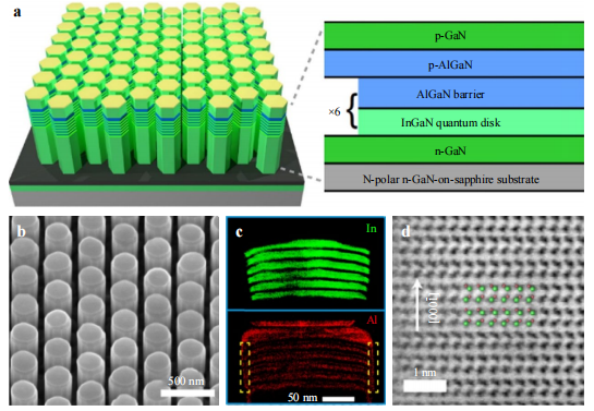
Taking advantage of these benefits, high efficiency Npolar green nanowire sub-micron scale LEDs have been demonstrated. To ensure the N-polarity of the grown nanowires, an N-polar GaN substrate was used for seeding the initial nanowire nucleation. Over a base n-GaN segment, a six-period InGaN quantum disk/AlGaN barrier active region was grown, followed by a p-type AlGaN electron blocking layer and a p-GaN contact layer. A schematic of the nanowires and their structure is shown in Fig. 4a. SEM images of the nanowires following growth confirm the uniform morphology and flat top surface, shown in Fig. 4b. Similar to studies on Ga-polar structures, an AlGaN shell was formed, protecting the active region from surface recombination. This was confirmed with elemental mapping of the active region, presented in Fig. 4c, for In and Al. High resolution atomic-scale images shown in Fig. 4d also confirmed the N-polarity of the grown nanowires.

Fig. 4
In polar semiconductors such as InGaN, the distinct ionic character can lead to strong electron phonon coupling effect, which may significantly impact their electronic, optical and excitonic properties. Recent theoretical and experimental studies have revealed that the exciton binding energy in nanoscale III-nitride heterostructures can be dramatically increased, compared to their bulk structures. As an example, the exciton oscillator strength can be enhanced by one to two orders of magnitude in InGaN nanostructures with efficient strain relaxation. Theoretical studies have further shown that polaronic exciton contribution to the binding energy can be as large as 190 meV in GaN nanowires. Moreover, recent studies have shown that the strong exciton-phonon interaction, i.e., the formation of polaronic excitons, can further impact the charge carrier transport, relaxation, and recombination. For example, the unique polaronic exciton effect can transform an indirect bandgap h-BN to be extremely bright light emitters in the deep UV. As such, we envision that a fundamental study of excitons in InGaN deep nanostructures could offer a path to break the efficiency bottleneck of micro and nanoscale LEDs.
The potential uses for micro-LED technologies have motivated considerable resources into their development. While obstacles remain in the path of nanostructure-based micro-LEDs, they can be solved by a fundamental understanding of the physics and properties of III-nitridenanostructures and the further development and refinement of the epitaxy and fabrication methodologies. Accordingly, III-nitride nanostructures offer a very promising path to overcome the efficiency, scaling, and integration challenges of micro-LEDs for many emerging and demanding applications.
上一篇: III-氮化物发光晶体管的设计