InGaN/GaN-based group-III nitride semiconductors are the most promising candidate materials for highly functional active photonic devices in the visible region. Low-damage nanoscale high-precision etching with vertical facets is important for realizing photonic crystal (PhC) and optically integrated devices. Herein, the etching characteristics of GaN nanoholes using the hydrogen environment anisotropic thermal etching (HEATE) method, which is based on the hydrogen-assisted thermal decomposition of GaN, are systematically demonstrated. It is found that high-precision and vertical nanofabrication is possible at high etching temperature (≈1000 °C) and low hydrogen pressure conditions (<18 Pa). In GaN-based visible topological PhCs composed of fine triangular nanoholes fabricated under these conditions, the photonic bands are observed to be in good agreement with the three-dimensional finite-difference time-domain simulations, indicating the effectiveness of the HEATE method.
1. Introduction
GaN-based semiconductors have been the subject of vigorous research and development for many years as light-emitting device materials that cover the entire visible light wavelength range.To improve the luminescence properties of these light-emitting devices and obtain new functionalities, various nanostructures have been introduced, including fine columnar structures,photonic crystal (PhC) structures,and distributed reflection type structures.Device structures using high-aspect and vertical nanostructures have also been proposed in electronic devices, such as vertical Fin field effect transistors and nanowire transistors.As indicated by these studies, GaN nanofabrication techniques with precise controllability, verticality, and low damage will undoubtedly become increasingly important in various device applications.
In the fabrication of GaN nanostructures, a bottom-up method using crystal growth and a top-down method using etching are generally used. Although the bottom-up method produces high-quality crystals, it relies on state-of-the-art crystal growth technologies and has reproducibility and controllability issues. The top-down method has good reproducibility and controllability; however, it has disadvantages such as difficulty in forming high-aspect structures of submicrometer size, the need for postwet etching to form vertical facets and remove serious physical damage during processing, and the need for expensive abatement equipment to treat toxic etching gas.
2. Results and Discussion
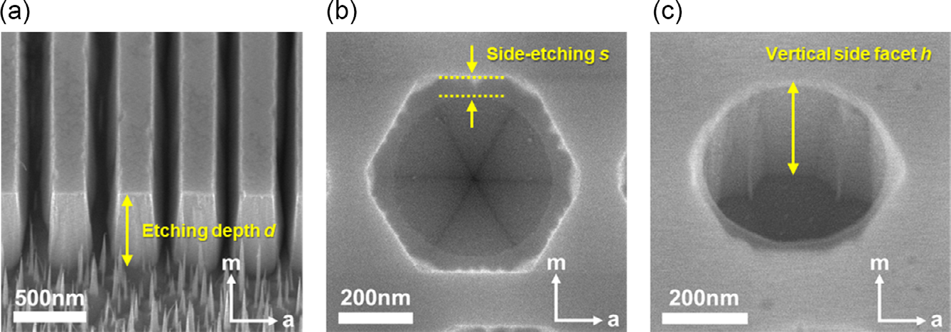
The effects of the etching temperature T and hydrogen pressure P, which are the two main parameters in the HEATE method, on the etch shape of the GaN nanoholes, were investigated. Three parameters–d, s, and h–were used to quantitatively evaluate the shape of the etch. In the HEATE method, the shape of the nanoholes was affected by the area and shape of mask aperture, in addition to T and P. To decide the standard of etching time for various etching conditions, we used the height of the stripe mesa structure “d” shown in Figure 1a, which does not depend on mask size and can be produced under all conditions. The value of d corresponds to the etching depth of the c plane in open space without the SiO2 mask. Schematic cross-sectional images of the etched structures are shown in Figure S1, Supporting Information. The side etching depth “s,” which is the distance of etching from the edge of the SiO2 mask, was used as an indicator of the shape error between the mask and the nanoholes, as shown in the scanning electron microscope (SEM) image in Figure 1b. The depth of the vertical side facets that appear at the periphery of the nanoholes is defined as vertical side facet “h,” as shown in the SEM image in Figure 1c.

Fig1
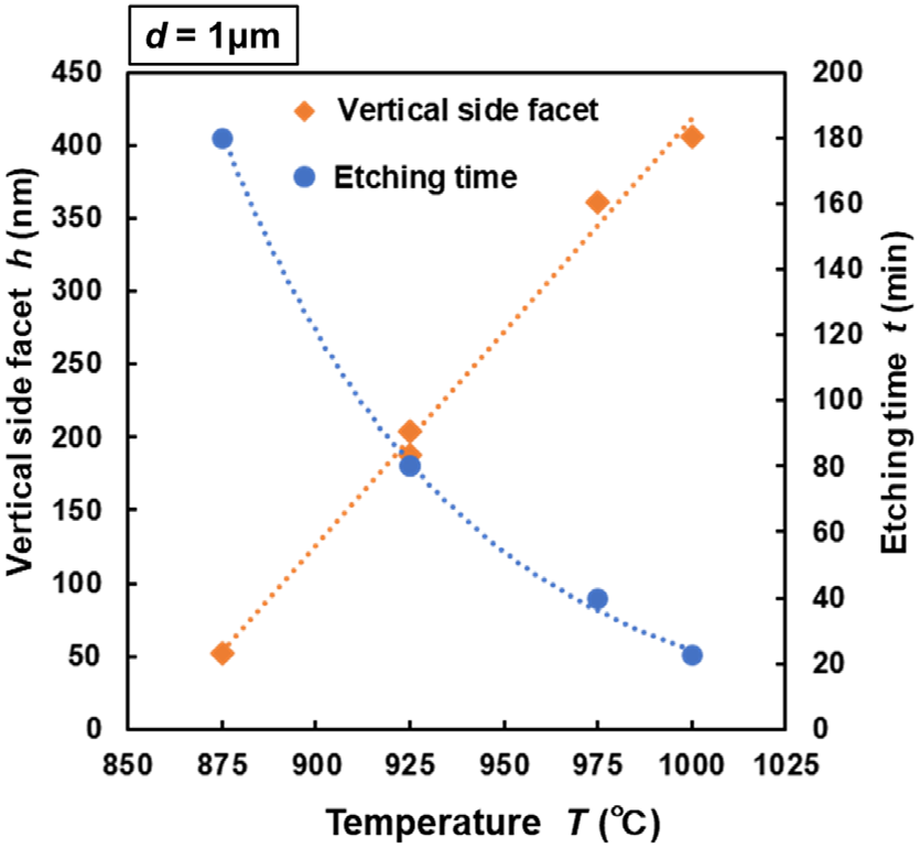
To evaluate the relationship between etching temperature T and nanohole shape of GaN in the HEATE method, we investigated the nanohole shape when etching T was varied (875, 925, 975, and 1000 °C) while hydrogen pressure P was maintained constant at 18 Pa. In all temperature conditions, the etching time t was adjusted to be d = 1 μm. Figure 2 shows cross-sectional bird’s eye-view SEM images of nanoholes etched using a hexagonal aperture mask at T = 875, 925, 975, and 1000 °C and P = 18 Pa (upper panels) and top SEM images of nanoholes etched using circular aperture masks (bottom panels). All the nanoholes had inverted hexagonal pyramidal bottoms consisting of six {1102} r planes whose angles to the c plane were ≈40°. The inclination angle was confirmed by SEM observations of the cleaved nanohole cross sections. Figure 3 shows the relationship between etching temperature T, etching time t, and vertical side facet h. Interestingly, despite maintaining d at 1 μm, the depth of the nanoholes varied significantly with temperature and h increasing at higher temperature.

Fig2
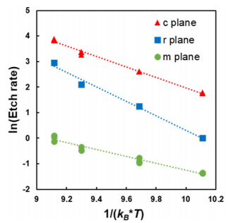
Figure 4 shows the Arrhenius plot of the etching rate (nm/min) for three crystalline planes at a hydrogen pressure of 18 Pa. For c and m planes, the corresponding etching values were d and s, respectively. For the r plane, the etching value was calculated in the direction normal to the inclined plane at the bottom of the nanohole. The etching rate was fastest on c plane and slowest on m plane, indicating that m plane was a stable plane with a slow etching rate. The activation energy Ea of each crystal plane was calculated from the slope of the graph, which were 2.1, 2.8, and 1.3 eV for c, r, and m planes, respectively. It can be inferred that the change in the nanohole depth h, despite a constant d in Figure 3, was caused by the difference in Ea between c and r planes. The SEM image in the lower panels of Figure 2, which used a circular mask, indicates that side etching s under the mask decreased as the etching temperature increased. The nanohole shape changed from hexagonal to circular, indicating that the difference between the mask and nanohole shapes decreased at higher temperatures.

Fig 4
3. Conclusion
The temperature and hydrogen pressure dependences of the etch shape of the GaN nanoholes were systematically investigated using the HEATE method with only hydrogen. It was quantitatively demonstrated that vertical etching facets with less side etching can be formed at high temperatures and low hydrogen pressures. GaN topological PhC membranes composed of modulated honeycomb-lattice triangular nanoholes with visible regions were fabricated using the HEATE method at an etching temperature of 1000 °C and hydrogen pressure of 18 Pa. The observed photonic band diagram was in good agreement with 3D-FDTD simulation results. These results indicate that the HEATE method with high temperature and low hydrogen pressure conditions developed in this study is an effective method for the fabrication of GaN nanostructures that require vertical etching of facets and precise shape control.
上一篇: 微型 LED 的最新进展
下一篇: 微流控芯片中微气泡聚集的表征