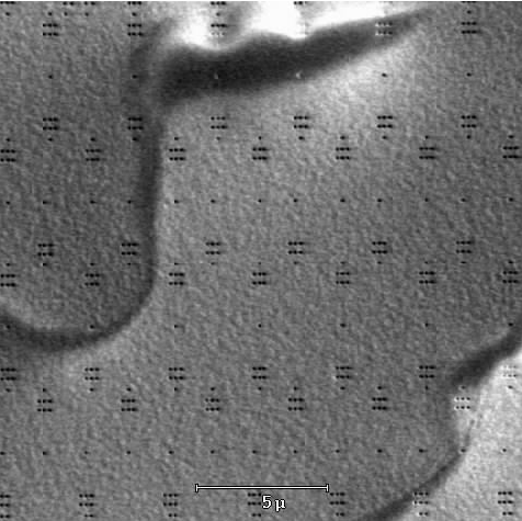
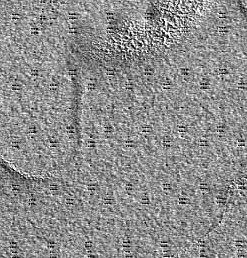
The objective of post etch wet clean is to effectively remove any post etch/ash residues from the wafer surface and inside the contact holes, in order to achieve low contact resistance. During wet clean, chemicals need to penetrate into the contact holes for reaction with any remaining post etch residues and these reaction by-products must be efficiently removed from the holes. The high aspect ratio of these holes would make it difficult for effective penetration and removal of residues, and could leave behind residues inside the holes, especially in a batch immersion system. This challenge could be further amplified when the wafers are processed at half pitch at 300mm. We have observed polymeric (CFx-based) residues extensively on wafers that are processed at half pitch during post etch wet clean with dilute SC1, which reveals the ineffectiveness of the cleaning process. This study aims to investigate the source of these residues and the mechanism behind their formation. It also reports the impact that drying techniques during the cleaning process might have on the resultant formation of these polymeric residues.
Logic devices with complete FEOL structures including STI, poly gate and Salicide,were fabricated on 300mm p-type silicon wafers with (100) orientation. After CVD deposition of the interlayer dielectric (ILD) films – nitride etch stop liner followed by oxide – contacts were patterned with 193nm ArF lithography. Subsequent dry etching to open up the contacts to the underlying silicide comprised of an oxide main etch followed by a nitride breakthrough etch, with different gas chemistries utilized for each step. In-situ ash using O2 followed the C4F6/O2/Ar oxide main etch, but no post etch treatment (PET) was employed following the CF4/CH2F2/Ar nitride etch. Remaining post etch polymers or residues were removed with wet clean using warm dilute SC1. The post etch clean utilizes point-of-use (POU) SC1 in a batch immersion tool, with surface tension gradient (STG) drying. Conventional TiN barrier metal and CVD-W was used for contact metallization. Defect inspection was done using a KLA2800 brightfield inspector and SEM review was done in an Applied Materials SEMVision review station.


上一篇: MEMS微加工中的真空辅助湿加工