Abstract— Wafer-to-wafer 3D integration has a potential to minimize the Si thickness, which enables us to connect multiple wafers with significantly scaled through-Si vias. In order to achieve this type of 3D structure, backside thinning is a key step. Conventional mechanical grinding is known as the best way to remove bulk Si in terms of cost of ownership (CoO). However, mechanical damage such as induced dislocations needs to be removed after extreme thinning to avoid a serious impact on the device performance. CMP shows the best performance in terms of roughness with a significantly flat surface with only atomic step roughness. Furthermore, the existing mono-vacancies are as low as for a bulk Si substrate. However the total thickness variation (TTV) worsens as more Si is removed. The dry etch process enables a faster etch rate than CMP and wet etching. Furthermore, the mono-vacancy/damage layer after dry etching is equivalent to that achieved when combined with CMP. The combination of CMP and dry etch enables us to achieve extreme thinning of active device wafers (<5 μm) with minimal roughness, no damage layer (mono-vacancy) and no edge delamination. Keywords-component; Edge-trim, Grinding, CMP, Dry etch, wafer-to-wafer bonding,
INTRODUCTION
Wafer-to-wafer stacking potentially offers a solution for thin wafer handling issues allowing the removal of most of the Si from the top wafer. The extremely thin Si (< 5 μm) can extend the scaling of via-last TSVs, due to the minimized pitch and dimension (pitch < 2 μm, dimension 1 x 5 μm). The via-last TSV formation is significantly influenced by the thinning performance, which brings new challenges in the thinning process [1]. A smooth surface and less damage into the Si are mandatory to achieve a successful backside TSV process. Accurate thickness control and minimal total thickness variation (TTV) across the whole wafer are required for the via etch process [2]. In particular, TTV is much more critical for the range of thin Si. In addition, any mechanical failures occurring at the very wafer edge, an area of the wafer typically excluded from inspection, may also impact multiple waferto-wafer bonding. Furthermore, vacancy-type of atomic defects need to be analyzed using depth profilinge for the extreme thinning, since the remaining Si is limited. Thus, adeeper understanding of micro and macro surface characterization is essential for extreme thinning. In this paper the characterization of different extreme Si wafer thinning processes are discussed on permanently bonded wafers. Several thinning methods, such as CMP and plasma dry etch are compared as subsequent processes of grinding. The wafer scale topography such as TTV, mean thickness control and wafer bowing will be discussed. The wafer inspections were performed up to the wafer bevel. In addition, nano-scale characteristics, such as roughness, mono-vacancies and damage in/to Si will be investigated by using alternative ways of surface detection.
EXPERIMENTAL
The thinning processes were performed on the top wafer of permanently bonded wafer stacks. The permanent wafer bonding was performed on 300 mm wafers. Oxide CMP is used to planarize and to smooth the oxide layer. Prior to bonding, the pairing wafers are treated with a combination of plasma activation and a DI water clean. Wafer bonding takes place at room temperature with atmospheric pressure in a clean room ambient. Then an annealing cure was used to improve the adhesion strength. The edge-trim process was performed using a dicing saw tool DFD6860 from Disco. The grinding step was carried out on a Disco DGF8560 series in-feed grinder which consists of rough and fine grinding wheels. The wafer nano-tomography was measured by a wafer automated inspection system. The wafer edge inspections were done in a KLA-tencor CIRCL-AP. The dry etching for Si thinning was performed by an SPTS Rapier XE system with Near Infra-Red (NIR) interferometer in-situ endpoint detection.

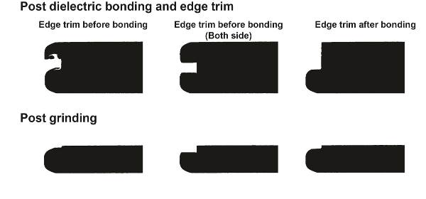
Figure 1. Wafer edge shadow images taken after edge-trim and grinding for different edge-trim approaches
A comparison of the damage into the Si was made between edge-trim before and after bonding. In order to compare the edge-trim impact cross-sectional TEM images were taken at the wafer edge after grinding. As the edgetrim depth after bonding is much deeper than for edge-trim before bonding, a blade with bigger diamonds is suitable for edge-trim after bonding. Figure 2 shows TEM images of dielectric bonded wafers after grinding using edge-trim before bonding (a)-(b) and after bonding (d)-(e). Dislocations and stacking faults in the {111} plane can be seen in the damaged regions in both samples. The presence of acontinuous amorphous Si layer was also observed at the wafer edge. The Si sidewall using edge-trim after bonding has a higher roughness, deeper defects (~500 nm) and thicker and continuous amorphous Si layer. This might be due to the transfer of a significantly big indentation and heat energy caused by the diamond abrasive process. The amorphous Si and different phases of Si are also detectable by using micro-Raman spectroscopy. Figure 2 (c) and (f) shows Raman spectra taken from the sidewall of the edge-trimmed Si. A lot of peaks can be distinguished for the case of an edge-trimmed sidewall. This indicates the temporary occurrence of significant high local stresses during blade dicing [3,4]. This does not create an immediate integration failure but these defects might represent the initiation of a fragile wafer edge.
上一篇: 使用臭氧技术去除光刻胶