We evaluated the trade off between damage generation and particle removal of single wafer aerosol spray and megasonic cleaning tools. This was done by the calculation of the local particle removal rates of 30 nm silica and the local damage fluxes of ~ 20 nm wide amorphous-Si lines. Cleaning and damage non-uniformities observed for aerosol cleaning were due to different exposure times to the spray nozzle. The non-uniformities for megasonic cleaning were due to different exposure times to the rod as well as to non-equivalent acoustic energy transmission across the wafer. Furthermore the extent of cleaning for equivalent damage generation was shown to be comparable for both techniques, but far from specification for the experimental conditions used here.
Damage tests were done with amorphous silicon lines (W/H/S = 20/65/1000nm) deposited on 150nm thermal oxide. Linewidth was monitored: 20 ± 3 nm, aspect ratio ~3. From lateral-force AFM measurements it was found that these structures are appropriate for damage tests (7). We also used gate stack lines composed of an SiO2 hardmask on top of poly-crystalline silicon deposited on top of SiON with an aspect ratio ~ 4 (W/H/S 40/160/1000nm) for comparison. Damage evaluation was done with KLA Tencor 2800. Damage adders were classified and quantified using Klarity and Impact software from KLA Tencor.
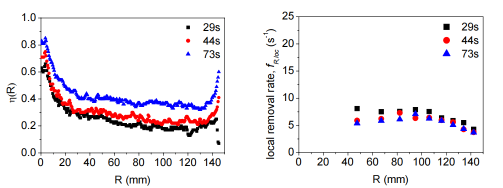
As a first illustration, a cleaning process making use of an aerosol spray nozzle moving across the wafer from edge to edge is characterized in more detail. The velocity of the nozzle increase from edge to center and decreases again from center to edge. The velocity change is linear in time. The cleaning solution was APM (1:4:20, 65° C) and rotation speed 1000 rpm. As can be seen in figure 2a, the local particle removal is much higher at the edge (R > 120 mm) and at the center (R < 20 mm) of the wafer. As explained in previous section, we calculated the local exposure time to the nozzle for different radii and extracted, by fitting, the local removal rate. Because the velocity change of the nozzle is very high at the center of the wafer, the exposure time calculation would be inaccurate at the center of the wafer. Therefore we did not calculate the removal rate for small radii. The results are shown in figure 2b.

The local removal rate, fR,loc was found to be rather uniform across the wafer compared to the the local removal efficiency. The apparent higher particle removal at the edge and center as seen in figure 2a is due to the longer exposure of these regions to the aerosol spray. Since no big differences were observed for different process times, see figure.2b, the model with constant fR over time (equation 4) is valid for this analysis. Also, the intrinsic particle removal rate was found to be rather uniform over the wafer, which confirms the stable nozzle performance. The particle removal rate for this aerosol spray condition lies around 6 s-1.
上一篇: 堆叠结构的晶圆及其减薄方法
下一篇: 蚀刻过程中砷在GaAs上的形成