III-V solar cell technology is important in space and concentrated photovoltaic (CPV) applications.1 From a fundamental point of view III-V semiconductors are ideal for solar cell applications. A large range of III-V materials are direct semiconductors allowing for thin- fifilm cell structures, and III-V compounds can easily be combined into multi-junction cells yielding record effificiencies.2 Present commercially available triple-junction cells for CPV systems reach effificiencies as high as 38%, while current research is aiming to demonstrate effificiencies above 50%. A major disadvantage in the production of high-effificiency III-V solar cells is that they require an expensive single-crystalline GaAs or Ge wafer as a template. After deposition of the solar cell structure the wafer is of no further use for its performance. Nevertheless, using the present fabrication techniques the active thin-fifilm structure including the passive wafer are processed together to a thick solar cell. In order to avoid wasting the substrate, our research group has perfected an epitaxial lift-off (ELO) technique to separate thin-fifilm solar cells from their wafer and transfer them to an inexpensive carrier. The ELO process involves the selective etching of an intermediate AlAs release layer, resulting in thin fifilm cell structures and thus allowing reuse of the wafer. Over the years this research has yielded signififi- cant increases in etch rate,3,4 an increase in sample size up to 4 inch wafers,4–6 thin-fifilm GaAs cells with record effificiencies (26.1%),7 and the demonstration of its potential for space applications.8 In recent years the importance of the ELO technology for PV applications has received wide-spread attention, resulting in further increase of the thin-fifilm GaAs cell effificiency to 28.3%9 and industrial interest for genuine thin-fifilm cell production.10–14 The aim of ELO is to allow the reuse of the wafer for the production of a large number of thin-fifilm cells with a minimum of wafer repreparation between consecutive deposition runs. It has been demonstrated that chemo-mechanical polishing of the wafers results in a series of consecutive thin-fifilm solar cells without any reduction in cell performance.6 However, chemo-mechanical polishing is a rather cumbersome process that reduces the wafer thickness by about 10 μm each time, thus decreasing the cost benefifit while limiting the number of wafer reuse cycles to 10 to 20.
Therefore, the use of a simple wet-etch procedure to clean the wafer after ELO is highly desirable. However, initial investigations showed that such procedures result in a serious deterioration of the performance of cells obtained from reused wafers, even when the wafers appeared clean and smooth to the naked eye after etching.6 Several studies were conducted to identify the actual residue thatmust be removed by the wafer re-preparation process.15,16 Because of the high etch selectivity of a HF solution for AlAs with respect to GaAs (∼106) 17,18 it was assumed that the residue only originated from the AlAs release layer. However, we recently observed that etching of GaAs wafers in a HF solution results in a surface with a brown haze similar to that observed on a wafer after ELO etching of the thin fifilm structure. This observation indicates that the residue after ELO (at least partly) results from etching of the GaAs wafer and not only from etching of the sacrifificial release layer. In the present study the mechanism of formation of the brown layer upon GaAs etching in a HF solution and subsequent evolution of the deposit during storage are studied in detail.


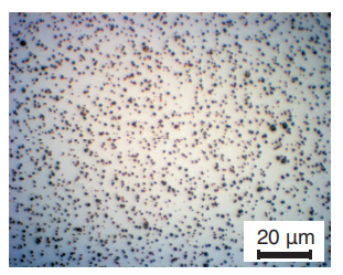
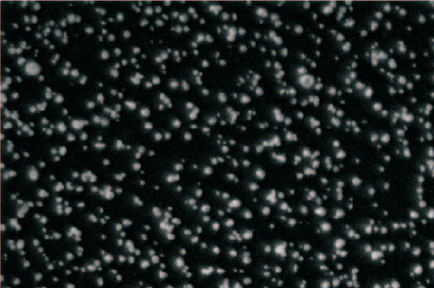
Figure 1. Optical micrograph of (a) the particles found on an etched and stored sample, and (b) after the corrected background intensity was subtracted from the image intensity (using an inverted greyscale).
CCD camera in differential interference contrast microscopy (DICM) mode was used. Samples were subjected to atomic force microscopy (AFM) analyzes using a Digital Instruments Nanoscope 3100 in contact mode with a Si3N4 tip. X-ray photoelectron spectroscopy (XPS) measurements were performed at the MESA+ Nanolab in Enschede, using a Quantera SXM with a base pressure <10−8 torr and an Al Kα monochromatic X-ray source. The measurements were carried out with an electron take-off angle of 45◦, unless otherwise specifified. With a take-off angle of 45◦ and the X-ray source used, one detects photoelectrons that originate from within the top 10 nm of the sample. During transportation to the XPS facility the samples were kept in vacuum and in the dark to avoid contamination and oxidation. The optical micrographs were analyzed for particle formation using a MatLab algorithm. The straightforward method of segmentation is to convert the image to grayscale, and subsequently separate the particles from the background by the difference in intensity (gray value). However, this does not take into account the non-uniformity of the background, for example as shown in Figure 1a, where the background at the center is brighter than at the edges of the image.
下一篇: 硅加工的高效清洁