Abstract.
The semiconductor industry is undergoing a transition driven by end use markets. In recent years, mobile devices have been the leading generator of growth. Now the connection of various products and machines to the internet is generating new and extensive demands for memory (storage of the data), logic (intelligent processing of the data including machine learning), and sensing (e.g., image sensors generating visual data). Thus the versatile planar MOS transistor based semiconductor technology has diverged into various specialized and complex branches, with each technology type using unique approaches to address scaling challenges. These lead to specific requirements for semiconductor wafer surface preparation. This paper will review the high level industry trends and how they affect surface preparation specifically.
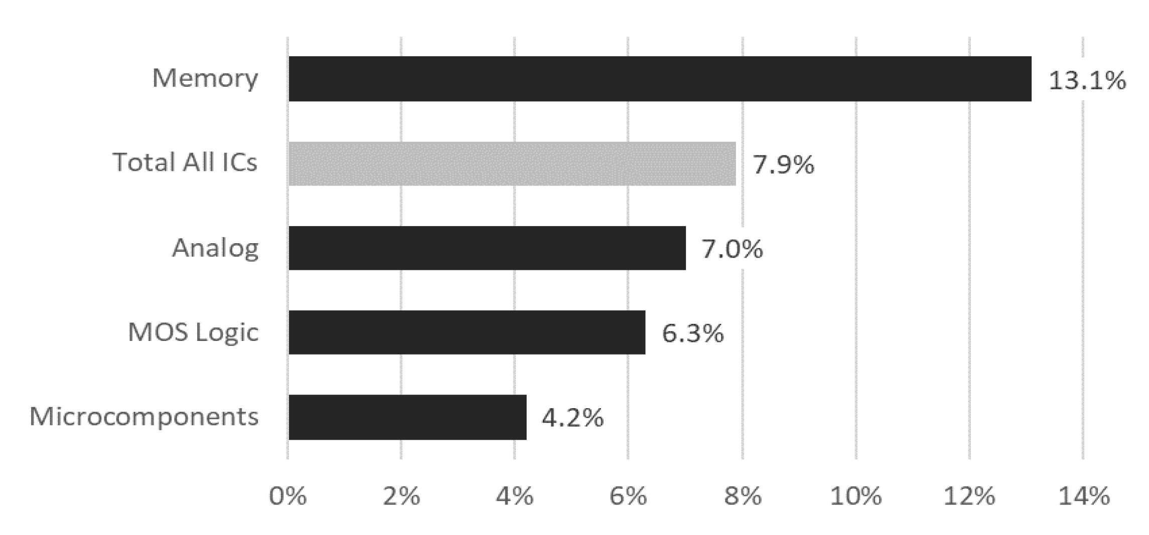
Introduction The world is continually being transformed by information handling systems that are enabled by semiconductors and the speed of their ongoing development. In turn, innovative and empowering applications are driving semiconductor technology development to continually overcome difficult barriers. With over half the world now connected to the internet [1], connectivity has begun expanding to various devices and machines transferring data and remotely storing it. With the expansion of this Internet-of-Things (IoT), many new and exciting capabilities are emerging. These include Virtual, Augmented, and Mixed Reality (VR/AR/MR), Artificial Intelligence (AI), autonomous driving, machine learning, Robotic Process Automation (RPA), and Blockchain. Associated massive amounts of generated data require fast local data reduction processing in combination with high volumes of memory storage, while high performance is required for machine learning and applications requiring minimal lag times (latency) such as autonomous driving and assisted surgery. The overall semiconductor market has been expanding in support of these emerging demands. Historically, from 1986 through 2017 this market has had a compound annual growth rate (CAGR) of 9%, becoming a $378B market in 2017. Even a more modest CAGR of 5% to 7% over the next 40 years would take it to $2.6T to $5.6T by 2057 [2]. As this market has matured in recent years the leading edge of semiconductor development has divided into a range of specific technology types, each having unique requirements. Enabling the various key functions in support of current and emerging end use applications are DRAM (working memory), NAND (information & data storage), MPU logic (supporting AI), and various sensors and actuators (e.g., CMOS Image Sensors, the visual component of automation). Dramatic growth in demand for memory has occurred, driven in large part by graphic and video applications in recent years [3]. The increase in photos taken every year is exponential, with a hundred billion more taken in 2017 than in 2016 (about 85% of these by smartphones) [4]. This trend is expected to continue. Figure 1 shows the associated high CAGR forecasted for memory revenue relative to other types of semiconductors over the years 2017 – 2022 [5]. This paper will review the evolution from planar technology to increased use of the third dimension in current semiconductor technology, and its relation to cleaning and surface preparation.

Figure 1: Forecasted compound annual growth rate (CAGR) of semiconductor revenue by product category for 2017 – 2022 (data from reference [5]).
In recent years, with the boom in demand for portable, non-volatile storage, NAND flash has come to represent a large share of the memory produced. NAND has a relatively low cost per bit, and while access times are much longer than DRAM or SRAM, NAND is much faster than Hard Disk Drives. These attributes have led to extensive use of NAND for SSD storage, and moved it closer to the goal of a non-volatile memory technology that can provide both short access times and low cost per bit. This category, known as Storage Class Memory, has seen much development in recent years [6-8]. Phase Change Memory (PCM) and Resistive RAM (ReRAM) are candidates for such Storage Class Memory. These various new memory candidates, plus others such as STT-MRAM, represent a division of the sector into diverse technologies having somewhat different requirements. Continued cost scaling to achieve higher bit densities has, along with surging demand, led to an expected 39% CAGR of NAND bit volume shipped in the period 2015 to 2020 [3]. To enable continued scaling of NAND in the face of fundamental limitations for traditional 2D layouts, major suppliers have introduced 3D NAND technology, with channels running vertically along pillars having memory cells at the intersection points of the pillars with horizontal layers that contain word lines [9]. Lithography dimensions become less critical and bit density is increased by adding more layers. Within 3D NAND there is also extensive customization, with the major producers pursuing somewhat different architectures and processing schemes. Current state-of-the-art 3D NAND uses 64 layers stacked vertically. Future cost scaling is expected to occur in the vertical direction with more layers, rather than the horizontal. Placement of the CMOS support functions under the 3DNAND memory array to conserve horizontal space has already been implemented [10]. Table I shows trends for scaling 3D NAND including number of tiers and critical dimensions (CDs). While the move from 2D to 3D increases bit density substantially, the bit density added per generation even for such aggressive increasing of tiers in 3D NAND is far less than what was historically realized per generation of 2D geometric scaling [11].
Table I: Scaling trend of 3D NAND devices by generation (adapted from reference [11]).

上一篇: 单晶片处理中的无损伤清洁
下一篇: 超细金属颗粒在硅片表面的行为