Abstract
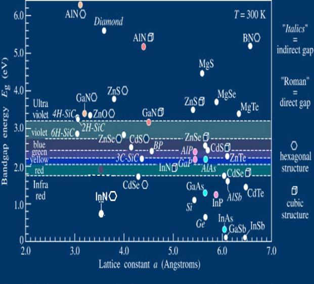
Silicon carbide (SiC) and gallium nitride (GaN) are typical representative of the wide band-gap semiconductor material, which is also known as third-generation semiconductor materials. Compared with the conventional semiconductor silicon (Si) or gallium arsenide (GaAs), wide band-gap semiconductor has the wide band gap, high saturated drift velocity, high critical breakdown field and other advantages; it is a highly desirable semiconductor material applied under the case of high-power, high-temperature, high-frequency, anti-radiation environment. These advantages of wide band-gap devices make them a hot spot of semiconductor technology research in various countries. This article describes the research agenda of United States and European in this area, focusing on the recent developments of the wide band-gap technology in the US and Europe, summed up the facing challenge of the wide band-gap technology.
Widely used of semiconductor technology in various military fields broke the traditional concept formed in thousands of years that weapons equipment’s advantage is only the size, the number and the more of massive destruction, so that system of weapons become smaller, lighter, less power wasted, higher reliable, stronger operational effective and powerful. Military electronic equipment required to operate at high temperature, high radiation and other harsh environments, can detect small targets of long-distance and real-time process high-speed sensor data, and the operating frequency band beyond the ordinary commercial range. Thus, require for the military electronic equipment for semiconductor components is much higher than ordinary electronic equipment, its safety and reliability of components must be higher. It is worth noting that, using conventional semiconductor technology to produce electronic systems has been unable to meet the requirements of next generation military applications for volume, weight and higher reliability. Wide band-gap semiconductor device has advantage of high frequency, high power, high temperature and potential of resistance to harsh environments, so that provides a method to solve these problem.

In the start-up and push of wide band-gap semiconductor technology program (WBGSTI) of US Defense Advanced Research Projects Agency, many other research projects of Europe ESCAPEE and Japan NEDO, SiC, GaN and other wide band-gap semiconductor materials and devices research gained rapid development; a number of international semiconductor manufacturers have introduced high-power, high-frequency, high temperature wide band-gap semiconductor products, whose applications are constantly expanded. In short, American and European countries will always put wide band-gap semiconductor technology on an extremely important strategic position, hesitate to invest heavily to implement a number of wide band gap semiconductor technology development plan in order to enhance the ability of military equipment, and have achieved good results. This article described the development of major initiatives in Europe and America in a wide band-gap semiconductor technology and the latest progress in the development and research in the device. It focused on the wide band-gap semiconductor technology development plan implemented in US, Europe and other developed countries and the far-reaching impact on military or other important facilities produce, summed up the facing challenge of the wide band-gap technology.
United States was the first country to start the wide bandgap semiconductor technology research, and many well-known universities and research institutions, such as Ray-theon, TriQuint, BAE, MIT, Cree, put a lot of manpower and material resources in the technology, and their research is most outstanding. DARPA hesitated to invest huge amounts of money to implement a number of wide band-gap semiconductor device and circuit technology development plans. DARPA aimed to enhance military radar, submarines and various other systems and equipment performance and reliability operated in harsh environment, and solved a number of technical bottlenecks of wide band-gap technology currently facing.
上一篇: 硅各向异性湿法刻蚀剖面演化的三维模拟
下一篇: 基于湿法刻蚀工艺的MEMS结构的研究