Abstract
In this paper, fabrication methods are developed in order to realize the silicon microelectromechanical systems components with new shapes in {100} Si wafers. Fabrication process utilizes wet etching with a single step of photolithography. The silicon etching is carried out in complementary metal oxide semiconductor process compatible pure and surfactant Triton-X-100 [C14H22O (C2H4O]n, n = 9–10) added tetramethylammonium hydroxide (TMAH) solutions. The fabricated structures are divided in two categories: fifixed and freestanding. The fifixed structures are realized in single oxidized silicon wafers, while freestanding are formed in silicon nitride-based silicon on insulator (SOI) wafers. The SOI wafers are prepared by bonding the oxidized and the nitride deposited wafers, followed by thinning and chemical mechanical polishing processes. The etching results such as {100} and {110}Si etch rates, undercutting at rounded concave and sharp convex corners and etched surface morphologies are measured in both pure and Triton added TMAH solutions. Different concentrations of TMAH are used to optimize the etching conditions for desired etched profifiles.
1 Introduction
There are two basic categories of etching processes: wet and dry etching. In micromachining technology, selection of the type of the etching depends upon the availability and requirement. In order to minimize the fabrication cost, which is the indispensable requirement of the industry, wetanisotropic etching is preferred over dry one. The {111}Si planes in the wet anisotropic etchants etch very slowly while all other crystal planes etch rapidly. Consequently, only rectangle and squares can be generated in {100} silicon wafers with a high degree of precision. The undercutting at mask edges that are not aligned along h110i directions on {100} Si surface is a well known characteristic of the wet anisotropic etchants. Thus, silicon wet anisotropic etching offers both advantages and disadvantages due to crystallographic limitations. For instance, formation of square shaped cavities, V-grooves, and suspended structures by undercutting are some of the advantages of wet etching for the development of MEMS-based devices. On the other hand, for the fabrication of MEMS structures including sharp convex corners and curved edges such as proof mass for accelerometer, circular grooves, serpentine microflfluidic channels, etc., wet etching is avoided owing to high undercutting at these types of corners and edges. However corner compensation method can be used to form the sharp convex corners, it cannot be used if structure includes rounded corners (or edges) (Pal et al. 2007a, b). In that case, only dry etching is the option as the etch rate is almost independent of crystallographic orientations (Bhardwaj et al. 1997). Moreover, CMOS process (or clean room) compatibility of etchant is also a serious concern especially when the etching step is attempted after the fabrication of CMOS circuitry. TMAH has gained wide popularity due to its clean room compatibility. In the last decade, different kinds of ionic and non-ionic surfactants are studied in TMAH to enhance the applications of wet etching in MEMS (Conway and Cunnane 2002; Jeon et al. 1996; Pal et al. 2007b, 2009; Resnik et al. 2005; Sarro et al. 2000; Sekimura 1999; Yang et al. 2005). The addition of a very small amount of surfactant in TMAH signifificantly reduces the etch rate of high index planes, resulting in a reduction of the undercutting at sharp convex,

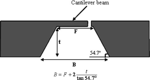
Fig. 1 Schematic view of wet bulk-micromachined suspended cantilever beams realized in {100} Si wafers using time-controlled backside etching
curved and non- h110i edges. Interestingly, these studies provide the choice to select the etchant according to the requirement of undercutting (e.g. high or low). Hence,TMAH (with and without surfactant) can be exploited to develop new processes/techniques for the formation of new shapes MEMS components in/on silicon wafers (Pal and Sato 2009a, b; Yang et al. 2005). In order to fabricate the freestanding silicon MEMS structures using wet bulk micromachining, the lithography as well as etching is performed on both sides of the wafer as shown in Fig. 1 (Abedinov et al. 2001; Wu et al. 1993). First the shape and thickness of the structures are defifined at the frontside of the wafer by photolithography and etching steps. Thereafter, the wafer is patterned on the backside with respect to the frontside patterns using a front-to-back alignment technique (Pal et al. 2006). In this case, the size of the backside patterns depends upon the wafer thickness (Fig. 1) and therefore, same mask cannot be adopted for different thickness wafers. Moreover, the silicon wet etching requires very time controlled in order to have tight control over the thickness of the released structures.
上一篇: 宽禁带半导体技术回顾
下一篇: 前端清洗工艺中的硅化物残留