Abstract— Salicide Residue is a common and well-known defect in CMOS technology of semiconductor wafer fabrication industries. This defect usually resides that is observed after Salicide Pre-Clean step whereby the product wafers after cleaning with standard diluted Hydrofluoric Acid (dHF). This defect can cause induced leakage current, directly impacting the electrical performance of the electronic product. Like many other wafer fabs, initiatives and efforts had been taken but never yield a very significant improvement. As of today, this type of defect is still persisting and remaining as one of the most challenging and unsolved phenomenon in wafer fabrication industry. This paper will explore next step towards eliminating the issues. Series of experiments were conducted to deduce the source to the root cause. Types of machines were screened through to dictate if the different machine hardware in general has significant contribution to the development of residue. Then the process tanks in the machine were tested to narrow the source of caused. The results of the experiments indicate a positive correlation between the DHF tank with the carbon residue after pre-salicidation clean which has lead the research to next step to solve the issue.
The advancement in the semiconductor wafer fabrication industry has been rapidly advancing. Semiconductor wafer fabrication also known as “fab” in short [1][2], is the most complex manufacturing process compared with other industries. The fabrication of semiconductor wafer requires the most advanced technologies in order to strive for the best among worldwide competitors. Wafers used in electronic integrated circuit (IC) fabrication usually in the size of round silicon disc consist of diameters ranging from 6”, 8” up to 12”[1]. The thickness of a single wafer disc is around 700um upon completed fabrication process before sending for wafer sawing process[3].
The new processes to accomplish each wafer fabrication with better resolution improved every year, in tandem with constantly changing technology in the wafer fabrication industry. New technologies result in denser packing of minuscule surface features. This increased density continues the trend often cited as Moore's Law [1][6][7][8].
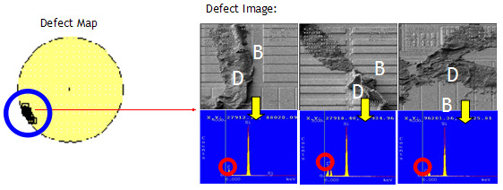
Wet cleaning plays an important part to ensure surface cleanliness for advanced semiconductor manufacturing process. As the technology node advances, it has become more and more challenging. Presence of organic residues and cluster of particles on product wafers can cause lot of issues. These clusters of particles and organic residues are found to be die killers and hence, reduce the yield of the product [11]. Residue defects affect the circuitry by causing a short between two neighboring metal structures. As the trend of maximizing the number of dies produced by a wafer, the physical size of a semiconductor die must reduce so that more dies can be accommodated on a single silicon wafer. Due to the significant deduction in size, this may cause two neighboring points become closer. Hence, any residue could have the potential to cause a short between two metal points thus affects the circuitry operation [12]. Salicide residue is a carbon defect which is observed after Salicide pre-cleaning step. The defect location is consistently seen at 7-8 o’clock region (with wafer notch at 12 o’clock during process) as shown in figure 1 below.

上一篇: 基于湿法刻蚀工艺的MEMS结构的研究
下一篇: 预氧化处理的影响