A wafer-scale graphene circuit was demonstrated in which all circuit components, including graphene field-effect transistor and inductors, were monolithically integrated on a single silicon carbide wafer. The integrated circuit operates as a broadband radio-frequency mixer at frequencies up to 10 gigahertz. These graphene circuits exhibit outstanding thermal stability with little reduction in performance (less than 1 decibel) between 300 and 400 kelvin. These results open up possibilities of achieving practical graphene technology with more complex functionality and performance.
Graphene, a layer of carbon atoms arranged in a hexagonal lattice, is a promising candidate for future high-speed electronics and radio-frequency (RF) applications (1–4) because of its high carrier mobility and saturation velocity (5). The planar structure and the feasi


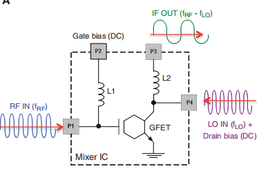
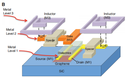
Fig. 1. (A) Circuit diagram of a four-port graphene RF frequency mixer. The scope of the graphene IC is confined by the dashed box. The hexagonal shape represents a graphene FET. (B) Schematic exploded illustration of a graphene mixer circuit. The critical design aspects include a top-gated graphene transistor and two inductors connected to the gate and the drain of the GFET. Three distinct metals layers of the graphene IC are represented by M1, M2, and M3. A layer of 120-nm-thick SiO2 is used as the isolation spacer to electrically separate the inductors (M3) from the underlying interconnects (M1 and M2).
vidual graphene transistor connected to external passive elements (11–13). Such heterogeneous circuitry inevitably results in degraded performance dominated by interconnects and parasitics rather than the intrinsic properties of graphene device. For example, Wang et al. demonstrated an RF frequency mixer operating at a few tens of megahertz based on a single graphene transistor (12). Despite recent progress in graphene synthesis and device performance, scalable integration of graphene into a practical circuit remains challenging. The key difficulties stem from the distinct materials properties of graphene with respect to those of conventional semiconductors, such as a different ohmic contact formation mechanism (14), poor adhesion with metals and oxides (15, 16), and its vulnerability to damage in plasma processing. Thus, bridging the technological gap between a single device and a practical graphene circuit on the wafer scale requires innovative integration processes and circuit designs. Here, we describe wafer-scalable processes that have been developed to fabricate arrays of graphene analog circuits, each consisting of one graphene transistor and two inductors, all compactly integrated on a single SiC substrate. The entire integrated circuit (IC), including the contact pads, is less than 1 mm2 ,

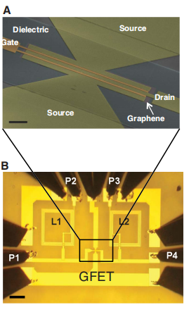
Fig. 2. Images of graphene ICs. (A) Scanning electron image of a top-gated, dual-channel graphene transistor used in the mixer IC. The gate length is 550 nm and the total channel width, including both channels, is 30 mm. Scale bar, 2 mm. (B) Optical image of a completed graphene mixer including contact pads. The gound-signal-ground configuration is implemented for the probe pads suitable for direct RF testing. Scale bar, 100 mm.
下一篇: 碳化硅的化学机械抛光