ABSTRACT
In an effort to improve silicon carbide (SIC) substrates surfaces prior to epitaxial growth, two chemomechanical polishing (CMP) techniques were investigated and the results were compared with a mechanical polishing procedure involving various grades of diamond paste. This work focused on silicon-terminated (0001) SIC surfaces.The two CMP techniques utilized (i) chromium oxide(lll) abrasives and (ii) colloidal silica polishing slurry. The best surfaces were obtained after colloidal silica polishing under conditions that combined elevated temperatures (—55°C) with a high slurry alkalinity (pH > 10) and a high solute content. Cross-sectional transmission electron microscopy showed no observable subsurface damage, and atomic force microscopy showed a significant reduction in roughness compared to commercial diamond-polished wafers. Growth experiments following colloidal silica polishing yielded a much improved film surface morphology
A pressing need in the development of SiC semiconductor technology is to improve the structural and surface quality of epitaxial films used in device fabrication. A flat and defect-free substrate surface is crucial for the epitaxial growth of thin films. Research on the epitaxial growth of 4H- and 6H-SiC has shown that processinduced defects on the substrate surface, such as scratches generated during lapping and polishing, are the primary contributors to unwanted polytype inclusions in the epi layer.14 Silicon carbide presents many challenges for wafer surface preparation because of its high hardness and remarkable chemical inertness. Existing surface polishing techniques for SIC can be categorized as purely mechanical, chemomechanical, or etching. Mechanical polishing of both poly- and single-crystalline SIC wafers primarily uses hard abrasives such as diamond polishing compounds mixed with water. Diamond abrasives achieve materials removal through plastic deformation, and thus unavoidably result in a hill-and-valley surface structure accompanied with a damaged (or strained) subsurface layer containing dislocations,5 although the surface roughness and the subsurface damage can be reduced significantly with the use of submicron sized diamond abrasive particles.6'7 In contrast, CMP techniques combine mechanical polishing with a chemical etching action, and can achieve truly defect-free surfaces. To the authors' knowledge, the only CMP process for SIC in the literature is a dry polishing process, reported by Kikuchi et al.,8 utilizing 0.5 m Cr203-impregnated acrylonitrile disks. These authors found an anisotropy in the polishing rate of 6H-S1C, with the rate of removal being significantly higher on the carbon-terminated (000T) face where they obtained a defect-free surface. Generally, the carbon-terminated face of SIC is considered not as useful as the silicon-terminated (0001) face for device fabrication or as substrates for film growth.The third approach to preparing a smooth surface is by etching. Similar to CMP, etching can completely remove any subsurface damage resulting from prior mechanical polishing steps. A process which may have produced probably the best on-axis Si-terminated (0001) SiC surfaces so far has been recently reported by Owman et al.9 These authors used an atmospheric-pressure hydrogen etch at 1550°C for 30 mm and obtained a defect-free surface with regularly spaced steps of single 6H-S1C unit-cell height. An obvious disadvantage of a purely etching method, as compared to a CMP process, is that the former is not a global planarization technique. Etching removes a uniform layer of material from surface, and therefore cannot efficiently reduce long-range roughness. CMP reduces both local and long-range roughness with careful selection of polishing pad material. In this article, we report successful CMP polishing of the Si-terminated (0001) surface of SiC using concentrated colloidal silica slurries at high pH values and at elevated temperatures. This process can be integrated with the necessary dicing and polishing procedure in SiC wafer production. It may also be useful in the planarization of SiC-based very large scale integrated (VLSI) multilayer devices and SiC-based precision ultraviolet (UV)-laser optics with which a high-temperature hydrogen etch is incompatible.

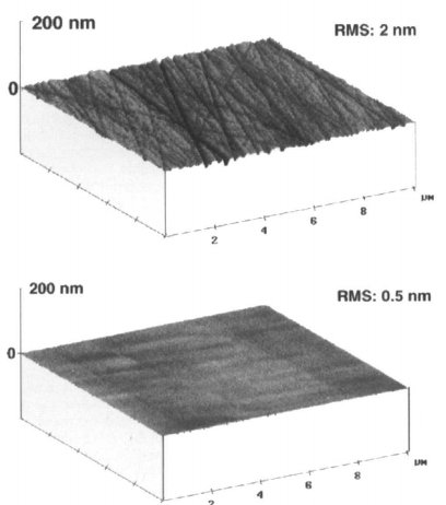
Fig. 2. AFM images of (0001) SiC surfaces showing effectiveness of colloidal silica CMP: (a, top) as-received commercial 4H-SiC wafer; (b, bottom) same area after CMP repolishing
上一篇: 晶圆级石墨烯集成电路
下一篇: 碳化硅与锗合金的电学特性