As an electronic material for high power, high voltage applications, silicon carbide (SiC) would be more versatile if suitableheterojunction partners were available. Using ion implantation, we have formed alloys of SiC with a few atomic percent olgermanium (Ge). The Ge was implanted at 346 keV and a dose of 1.67 x 10' cm- into a p-type 4H SiC wafer at roomemperature, and followed by subsequent annealing up to 1700°C. Through X-ray diffraction (XRD) measurements it wa?determined that the Ge implanted SiC had a larger lattice constant which implies that some of the Ge is substitutional. The Xray measurements indicated that a secondary peak attributable to substitutional Ge increases in intensity and shifted toward aower Bragg angle as the implanted Ge dose was increased. SiC/SiC:Ge heterojunction devices were formed using titaniumgold (Ti/Au) as electrical contacts. Current-voltage (L-V) and capacitance measurements confirmed a reduction of the forwarovoltage drop and buil-in voltage in SiC:Ge, compared to similar SiC devices without Ge. Other p-type substrates implantedwith Ge that used chromium/ickel (Cr/Ni) metalization as electrical contacts were shown to have a signilicantly lowercontact resistance compared to SiC. These results indicate that the SiC/SiC:Ge material svstem may be promising for Sicheterojunction device applications. C) 2001 Elsevier Science B.V. All rights reserved.
Rutherford backscattering spectrometry (RBS), X-raydiffraction (XRD), current-voltage (1-V), and capa-citance-voltage (C-V). The SiC:Ge films were createdby ion implantation into a p-type 4H SiC wafer fromCree Research doped p-type to 5 x 1016 cm-3. Thewafer was at room temperature during the ion implan-tation process. Approximately half of the wafer wasimplanted with nitrogen (N). The N implantationwas performed in a series of four steps to achieve auniform N profile in the wafer. The final N implantwas from a 124 keV ion beam source with a dose of

9.0 x 1014 cm-2, which gave a highly doped n-typeregion having a peak concentration of 1 X 1020 cm-3After rotating the wafer by 90°, it was implanted withGe to approximately 8 x 1020 cm-3 from a 346 kevion beam with a dose of 1.67 x 1016 cm-2. Thisresulted in a wafer of quadrants with surface layersof SiC, with and without Ge and N. The projected ionrange and longitudinal straggle values calculated withthe SRIM program for the implanted ions are providedin Table 1 [l]. The implantation depths were con-firmed with secondary ion mass spectroscopy (SIMS)which agreed well with the SRIM calculations andindicated similar depths for the Ge and N implants.After implantation, the substrate was annealed in stepsup to a maximum temperature of 1700°C for 20 min.
2. Experimental results
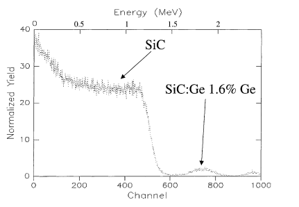
The RBS data was obtained with a 2 MeV He' ionaccelerator, for both the SiC and the SiC:Ge regions ofthe substrate. The data was compared to theoreticalcalculations using the Rutherford universal manipula-tion program (RUMP) [2]. The RBS data in Fig. 1showed evidence of the underlying SiC substrate, theSiC:Ge surface layer, and a thin region of metalizationon the surface from the electrical contacts. RUMPsimulations yielded a SiC:Ge layer thickness of2700 A with a peak Ge concentration of 1.6%. Thisamount of Ge was also obtained in previous studies ofsiC:Ge。

Fig. 1. RBS data from the SiC:Ge layer showing evidence of C, Si.and Ge profiles. The data was taken with a 2 Mey He+ RBSsystem. The SiC RBS profile is evident below 1.2 MeV where theHe* ions are scattered from Si atoms. C atoms in the SiC cause theincreased scattering below 0.5 MeV. The Ge profile is seen at1.8 MeV and a thin layer of heavy metal atoms causes the smallpeak at 2.4 Mev.
上一篇: 碳化硅的化学机械抛光
下一篇: 先进材料抛光的最新进展