Metal contamination is the dominant cause of device failure. In the case of an epitaxial (Epi) wafer, trace metal may well be in the bulk as well as on the surface. Generally, we can analyze it in the bulk using Surface Photo Voltage (SPV) or Micro-Photo Conductance Decay (µ-PCD), but the metal contamination in an epi wafer on a heavily doped substrate, for example p/p+, cannot be measured by those methods. We can analyze the metal contamination in the bulk using the photoluminescence (PL) and local etching Inductively Coupled Plasma Mass Spectrometry (LE/ICP-MS). The PL technique at room temperature is applied to evaluate the metallic contamination in the epi layer and the epi substrate, and the LE/ICP-MS can offffer us the qualitative and quantitative results on infifinitesimal metal contamination. We can also get the depth profifile of the trace metal in epi wafer (p/p+) by using those methods. In this paper, we explain the effffect on the device of infifinitesimal metal on an epi substrate.
Keywords: Epitaxial wafer, Metal contamination, Depth profifile, PL, ICP-MS, Si, Cu, Ni, Fe
I. INTRODUCTION
Both crystal defects and metal contaminations are presumed to be causes of device failure. With the reduction in the design rule in ultra-large-scale-integrated (ULSI) silicon technology, it is very important to eliminate those causes [1–3]. Silicon wafers with epitaxial grown fifilms have been widely used in the semiconductor industry to manufacture bipolar transistors and advanced CMOS ULSI devices with improved electrical performance [4, 5]. The epitaxial layer can be made free of oxygen and carbon and with well-controlled dopant concentrations, and a perfect crystalline structure can be achieved. In addition, the epitaxial layer is made free from the crystal originated particles (COPs) that are common with non-epitaxial silicon wafers [6]. Metal contaminations, more than crystal defects can detrimentally affffect the performance of microelectronic devices on the epitaxial (epi) wafers more [7]. Thus, it is of great importance to evaluate whether solubility or segregation-induced gettering mechanisms can describe the reaction pathways of a trace metal in silicon. A trace metal in a silicon wafer may well be in the bulk or on the surface. Both surface and bulk techniques are commonly used for monitoring metal contamination in wafer processing. Surface techniques, such as total reflflection Xray flfluorescence spectroscopy (TXRF), time-of-fifight secondary ion mass spectrometry (TOF-SIMS) and vaporphase decomposition- Inductively Coupled Plasma MassSpectrometry (VPD/ICP-MS) are generally suitable for the detection of surface-deposited contaminations. On the other hand, these techniques usually provide a limited mapping capability only, and they are unsuitable in the case where contaminations are diffffused into silicon, as may happen when contamination is introduced by using an epitaxial growth procedure, thermal treatment or device process. The bulk analysis methods, such as the lifetime technique, deep level transient spectroscopy (DLTS), or dynamic secondary ion mass spectrometry (D-SIMS), are suitable for the detection of bulk contamination [8,9]. The carrier lifetime is related to the metal contamination. A microwave-detected photoconductive decay (µ-PCD) and a surface photovoltage (SPV) are frequently used as methods to measure the lifetimes in silicon wafers without making any special test devices [10, 11]. They are, however, not applicable to lifetime measurements in p/p+ silicon epitaxial wafers because of the heavy boron doping in the substrates. The photoluminescence (PL) technique can be used for non-contact characterization of silicon wafers and has been employed for a long time. In particular, analysis of the PL spectra for deep level assisted PL at liquid helium temperature was found to be very effffective for defect identifification [12, 13]. The room-temperature PL technique also has great practical advantages, such as high sensitivity, high spatial resolution, non-destructiveness, and no need for special sample preparation [14].
In this paper, we report a novel technique, the PL technique at room temperature, which has been designed to evaluate the metal contamination in the bulk of an epitaxial wafer. Also, additional sample preparations forCharacterization of Bulk Metallic Contamination in· · · – Sangwook Wee et al. -1161。


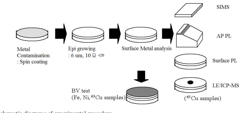
Fig. 1. Schematic diagrams of experimental procedure.
obtaining depth profifiles by using both PL and ICP-MS are introduced. The D-SIMS technique is the most popular method to measure trace metal in the bulk silicon. However, in this study, it could barely detect infifinitesimal metal contamination occurring during the wafering and epitaxial layer growth process. We also provide insight into the movement of metal impurities in an epi wafer. The origin of metal contamination is on the surface of substrate. Metal impurities are driven into the epi wafer during the epitaxial growth process without any additional diffffusion process.
上一篇: 使用稀 HCN 水溶液清洗SiC 的方法
下一篇: 无氧化物硅的湿化学表面功能化