Abstract
Cost-performance advantage of electrochemical processing technologies has enabled a paradigm shift in chip making. The dual Damascene process for Cu chip metallization and the C4 (flip-chip) technology for area array chip-package interconnection have placed electrochemical technologies among the most sophisticated fab processing technologies. These processing technologies have now been integrated into 300 mm wafer processing facilities for chip fabrication. New materials and processes are continuously being developed to meet the microprocessor industry’s increasing performance and miniaturization trends. Electromigration issues, and the need for novel polishing approaches to integrate ultra low-k dielectric materials with Cu metallization are some of the immediate concerns in chip making. Development of a compliant, cost-effective Pb-free C4 chip-package interconnection is another key objective of the microelectronics industry, which is making an effort to market Pb-free products in few years. All of these developments provide ample opportunities for electrochemical processing technologies. # 2003 Elsevier Ltd. All rights reserved.
Keywords: Chip fabrication; Microprocessor; Electrochemical processing technologies; Cu metallization; Flip-chip technology; Dual Damascene electroplating; Area array chip-package interconnection
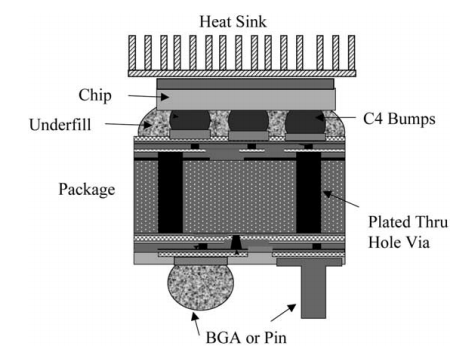
Introduction During the past decade, electrochemical technology has played a decisive role in the phenomenal advancement and growth of storage, interconnection, packaging and other aspects of the microelectronics industry. Due to its efficient cost-performance capability, electrochemical processing has now emerged as a technology of choice for the manufacturing of a variety of electronic components from ‘‘low-end’’ consumer products to advanced ‘‘high-end’’ microprocessors. In the present paper the impact of electrochemical technology in microelectronics is discussed using an example of the fabrication of microprocessors. Fabrication of chips, and their interconnects constitutes the high-end spectrum of the microelectronics industry, where specifications for increasing performance and miniaturization keep on changing every 18 months. New materials and processes are being developed to meet the industry’s performance and miniaturization goals and the trend is expected to continue [1]. The challenges associated with these foreseeable developments are providing tremendous opportunities for electrochemical processing technologies. Electrochemical processing technologies employ both metal deposition and dissolution processes. One of the essential requirements of electrochemical processing is the presence of a continuous layer (seed layer), which conducts electric current from the wafer edge contact to all points in the wafer where deposition/dissolution is desired. Three different types of electrochemical wafer processing techniques applicable in the fabrication of a metallic structure are, (i) through-mask plating; (ii) Damascene plating; and (iii) through mask etching [2 / 4]. Damascene Plating is another version of patterned plating, which brought about a revolution in the fabrication of chip interconnect and in electrochemical processing. In Damascene plating, the patterned dielectric remains intact and forms a functional part of the structure. A continuous seed layer conformally covers the patterned dielectric. Plating occurs all over thesurface thus creating challenges for void-free structure fabrication [3]. Chemical mechanical polishing (CMP) is used for planarization and removal of excess ‘‘overburden’’ metal, and seed layers. All of these three methods are employed in the manufacturing of advanced microprocessors and microelectronic packaging components. Fig. 1 is a schematic diagram showing the key components of a microprocessor assembly [5]. The assembly consists of chip, package, chip-package interconnects, and heat sink. Chips with solder bumps are flipped over and joined to the package substrate by reflow. An underfill is often used to improve reliability of the interconnect assembly. Also shown in the Fig. 1 are ball grid arrays (BGA’s) and pins for further connection of the assembled package to boards. A heat sink is attached to the backside of the chip for efficient heat dissipation. Electrochemical processing technologies, employed in the fabrication of all of these components, vary from low-end electroless gold coating of the copper heat sinks to the fabrication of extremely precise nano-scale features of chip interconnect metallization. Accordingly, the degree of sophistication of tools and processes vary based on whether they are applied in package fabrication or in wafer fabrication. The present paper discusses the impact of electrochemical technologies on semiconductor wafer processing of chip metallization and chippackage interconnection. Fig. 2 shows a simplified picture of microprocessor components fabricated on silicon wafers. Silicon wafers are generally 500 /800 mm thick. Leading chip manufactures currently use 300 mm wafers that can accommodate in excess of 500 chips. Transistors and other devices are fabricated on these Si wafers using the socalled ‘‘Front End’’ operations. A single chip (1 /1 cm) these days contains hundreds of millions of such devices that are 50 /500 nm thick. Indeed, Intel’s latest 90 nm technology will pack 330 million transistors in an area measuring only 109 mm2 [6]. These devices are connected by an efficient wiring layout consisting of a stack


上一篇: 无氧化物硅的湿化学表面功能化
下一篇: 硅片水处理过程中监测金属污染的方法