Keywords: heterojunction, texturization, PECVD
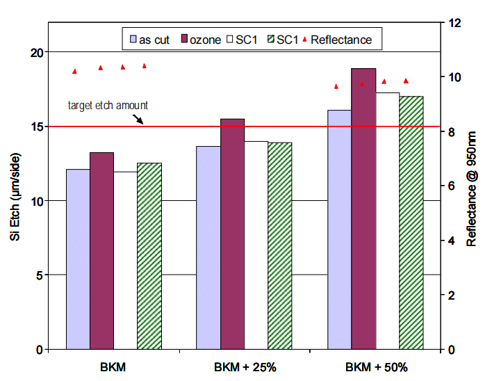
Introduction The semiconductor industry considers wet cleans to be critical surface preparation steps. The Si/SiO2 interface, for example, is very critical to achieve high gate oxide integrity and avoid leakage or stacking faults. Similarly, the solar industry has seen the value of wet processes to achieve best cell performance. In this study, we highlight the effect of pre-cleans, texturization and final cleans on cell parameters. We also studied the importance of coupling these wet cleaning and texturization steps with the PECVD steps to achieve the film quality required for highest solar cell efficiency. Experimental Wet chemical processes were conducted on a fully-automated GAMA Solar™ etching and cleaning station. Mono-crystalline n-type wafers were used for this study as part of HIT solar cell development efforts. Wafers were pre-cleaned in DIO3™ or SC1 and then texturized in a standard KOH/IPA process. In certain runs, proprietary process was applied to round the pyramid's peaks. The wafers were then processed in an advanced HF/HCl step prior to placement in the PECVD tool. Different PECVD splits were conducted to develop optimum process conditions. Results and Discussion Heterojunction (HIT) cells and n-type wafers are getting more traction as a technology to achieve the industry's goal of developing high efficiency, low cost solar cells [1,2]. Sanyo and Sunpower have been using n-type wafers for many years. Recently, all major R&D centers and several companies have published articles about using n-type wafers, which generally have higher lifetimes than p-type silicon, for cell processing. N-type wafers' long diffusion length and high lifetime result in higher cell efficiency, while boron-doped p-type wafers show lifetime degradation due to formation of boron-oxygen defects upon illumination [1-4]. We studied the effect of surface conditioning and the coupling of these surface preparation techniques and PECVD processing to produce high efficiency solar cells. A. Effect of Pre-cleans Various pre-clean processes were tested to determine their effect on the texturization step. Several wafers were processed in DIO3 and SC1. The results showed that the wafers processed in DIO3 consistently gave a higher Si etch (Figure 1). The wafers also looked more uniform visually, with fewer fingerprints and scratches. SC1 did not show any significant advantage over the as cut wafers. Reflectance at 950 nm wave length for all wafers processed for BKM+50% was <10% (>10% at BKM conditions).

Figure 1: Si etch and reflectance versus various pre-clean processes.
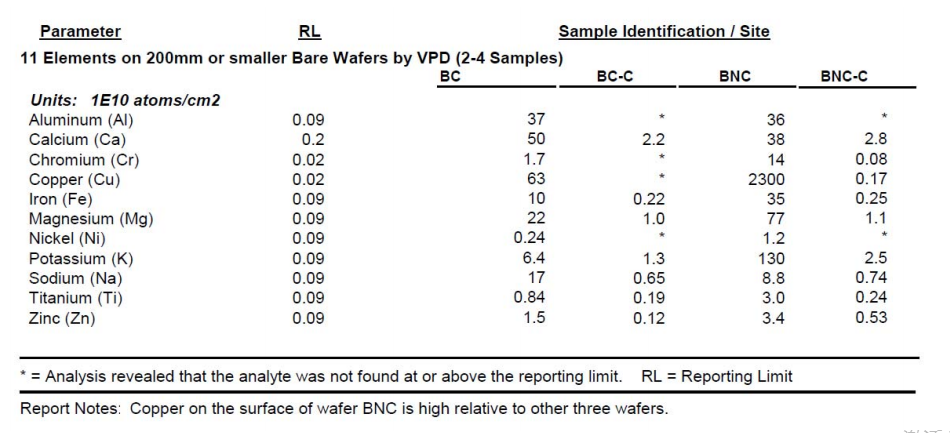
Table 1: Surface metal levels after different final cleans using standard and modified HF/HCl mixtures

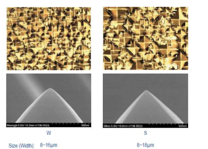
B. The effect of Final cleans Special attention has to be made to the final clean prior to PECVD. Typical tools in solar lines leave metal signature on the wafers that is responsible for low minority carrier lifetime. High levels of metals on production wafers in an advanced fab from two different production tools are shown in Table 1 (splits BC and BNC). A specially designed HF/HCl process was applied to the wafers that resulted in significantly lower metals on the wafers’ surface as can be seen from Table 1 (splits BC-C and BNC-C). Higher lifetime values (> 1000 µs) were obtained on these wafers after the special HF/HCl step. C. Effect of PECVD Deposition Conditions These factors were considered when processing the W, S, and C wafers. S wafers were slurry wire-cut while C and W were diamond wire-cut. Wafers were textured in the standard KOH/IPA process and no rounding step was done. The texturization pattern and pyramids shape are shown in Figure 2. Wafers from both W and S types were processed Si Etch (µm/side) Reflectance @ 950nm Si Etch (µm/side) Reflectance @ 950nm Si Etch (µm/side) Reflectance @ 950nm Si Etch (µm/side) Reflectance @ 950nmat the same time. Yet, the pyramid bases were larger for S wafers than those obtain for the W wafers.

Figure 2: pyramid patterns after standard KOH/IPA texturization for different wafer types (slurry and diamond-cut).
Further optimization of the standard texturization process produced a relatively smaller pyramid base and data is shown in Figure 3. The base of the W wafers ranged from 7-15 µm and the S wafers ranged from 6-15 µm. Another group of wafers was tested as well (wafers C) whose base ranged from 7-17 µm. A secondary process was then conducted on all the wafers to round the sharp peaks of the pyramids for better film deposition and conformity. The results are also shown in Figure 3. For optimum PECVD i-layer deposition, the desired radius of curvature was ~10 µm. Table 2 shows the results of the different PECVD processes used for optimization. Lifetime and Voc were measured. Voc is the open-circuit voltage - the maximum voltage available from a solar cell which occurs at zero current. As expected, the Voc, is directly related to cell lifetime: the higher the lifetime, the higher the Voc for any wafer and any process. The data also show that different PECVD processes produce different results for lifetime and Voc for the same wetprocessed wafers. Therefore, it is important then to tune the PECVD to match a wet process that produces well-texturized and clean wafer in order to maximize the Voc. In addition, the results in Table 2 also show that pyramid rounding further enhances the minority carrier lifetime and Voc. Table 2: Effect of PECVD deposition conditions on the minority carrier lifetime and implied Voc.
上一篇: 硅片水处理过程中监测金属污染的方法