Introduction
1.1. Conventional electroless plating Electroless plating refers to the autocatalytic or chemical reduction of aqueous metal ions and subsequent plating onto a substrate. In this process, metal ions are reduced to metals by reducing agents that are simply electron donors and the metal ions are electron acceptors which react with the electron donors. The catalyst is the sample which accelerates the electroless chemical reaction allowing oxidation of the reducing agent. In order to facilitate electron transfer, both the metal ions and reducing agent must adsorb onto the catalytic surface. The metal ions take part in the reaction in the form of charged ionic complexes. Unlike electroplating, no electrical current is required for deposition, but the substrate being plated must be catalytic in nature. A properly prepared substrate provides a catalyzed surface, and after introduction into the electroless solution, uniform deposition commences. Minute amounts of the electroless metal such as nickel, copper, etc. catalyze the reaction and so deposition is autocatalytic after the original surfaces are coated. Afterwards, electroless deposition continues, provided that the metal ions and reducing agent are replenished. However, it should be noted that the exact chemical mechanism of electroless plating is rather complicated and still remains a point of controversy. Electroless plating is a widely used method to metallize surfaces. Using electroless plating baths, a variety of metals such as Cu, Ni, Co, Pt, Pd, Au, Ni/Co, Pb, and Sn can be deposited. The most widely used electroless plating process is electroless nickel. Electroless nickel offers unique properties including uniformity of the deposit in deep recesses, bores, and blind holes. Electroless nickel plating was fifirst proposed by Brenner and Riddell [1,2]. Their work led to a process capable of plating the inner walls of tubes with nickel–tungsten alloy by means of an insoluble anode and brought out the unusual reducing properties of hypophosphites. In 1947, Narcus published the fifirst paper on electroless copper plating [3], and the fifirst commercial application of electroless copper plating was reported by Cahill in 1957 [4]. Electroless copper deposition is generally applied before electroplating on plastics and other nonconductors to provide a conductive base for subsequent plating. The electroless copper process improves the lifetime and performance in a corrosive atmosphere and upon exposure to a harsh environment. Electroless gold is currently being used in the fabrication of semiconductor devices, connector tabs, chips, and other metallized ceramics. Electroless palladium is ductile and ideal for contacts needing flflexing, for instance, printed circuit board end connectors and electronic switch contacts. It has also been used as a less expensive replacement for gold to provide tarnish resistance and solderability. Similarly, thin electrolesscobalt is used on magnetic memory disks and storage devices primarily for their magnetic properties. In nanotechnologies, electroless plating is widely used in lithography and rapid prototyping. This technology allows one to produce photo masks and micro-devices with nano-size adjacent elements of different thicknesses made of various materials by conventional optical photolithography [5]. These metallic micro or nanostructures are useful in many practical applications including regular porous metal materials in photonic crystals, micro-reactors, separation fifilters, and so on. They have been prepared by not only top–down lithographic methods, but also bottom–up processes. The technique is simpler than other expensive and complicatedmethods such as electron beam or X-ray lithography and phase shift photo masking. Methods to fabricate ultra-thin, void-free, and pore-free coatings onmicro,meso, and nanoparticles such as carbides, borides, nitrides, oxides, diamond, graphite, zeolites, and so on using electroless plating have also been developed. These methods also allow one to obtain nanostructured composite materials and coatings with specifific properties, for instance, metal-coated fullerences, metallized carbon nanotubes, conductive nano-size additives to plastics and rubber, nanoparticle reinforced tires, sensors, detectors of chemical and biological agents, unique catalysts, adsorbents, and hydrogen storage materials.
1.2. Metal-assisted electroless etching 1.2.1. Porous semiconductors In conventional electroless plating, the base substrate provides a catalyzed surface that is protected from etching. In 2000, Li and Bohn demonstrated a metal-assisted electroless etching method to produce light-emitting porous Si [6]. Porous Si is of interest due to their potential applications to optoelectronics. There have been three electrochemical routes to produce porous Si, namely anodic etching, photoelectrochemical etching, and laser-assisted etching, and all three processes are conducted in acidic flfluoride solutions. A thin layer of Au, Pt, or Au/Pd is deposited on the Si surface prior to immersion in a solution of HF and H2O2. Depending on the type of metals, Si doping type (n- or p-type), and dopant concentration, porous Si with different morphologies and light-emitting properties have been produced. Studies suggest that thin metal coatings facilitate etching in HF and H2O2 and a reaction scheme involving local coupling of redox reactions can explain the metal-assisted etching process. This technique has been extended to the electroless fabrication of patterned nanocrystalline Si. Compared to conventional electroless plating, two different points regarding metal-assisted electroless etching should be noted. First of all, the substrate does not serve as the catalyzed surface but rather electron donors, so that it can be etched to form the nanostructured patterns.

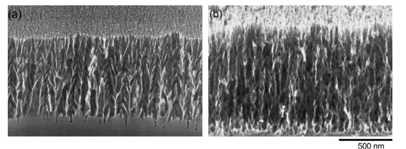
Fig. 1. Cross-sectional scanning electron microscopy (SEM) images (308 tilt) of porous GaN structures produced by Pt-assisted HF/H2O2 etching of n-GaN/SiC for: (a) 15 min, and (b) 40 min. The depth of the
下一篇: APCVD沉积的低温二氧化锡薄膜