Abstract
Electrochemical etching of silicon in hydroflfluoric acid (HF) solution is employed as a micromachining technique. It is demonstrated that the commonly accepted geometric constraints on the shape of electrochemically etched silicon structures can be signifificantly relaxed. Several new structures etched on the same n-doped silicon wafer are reported. The fabricated structures include wall arrays, hole arrays, meander-shaped structures, spiral-like walls, microtubes, micropillars, microtips and more. A simple model for the electrochemical etch process, which describes the effect of the dimension of the initial seed, the current density, and also the KOH etching time of the initial pattern on the fifinal geometries, is detailed.
Introduction
Electrochemical etching of silicon in hydroflfluoric acid (HF) electrolyte is a well-known technique for the formation of porous silicon [1]. Depending on the doping of the anodized silicon substrate, different pore morphologies can be obtained, ranging from nanometric pores made from p-type substrates, to micrometric pores obtained from illuminated n-type substrates. In the last case, by illuminating the rear surface of the wafer with suffificiently energetic photons, holes can be photogenerated in the bulk. Under anodic bias, these holes move toward the front silicon– electrolyte interface and silicon dissolution takes place. Initially, the electric fifield concentrates at sharp defects on the flflat wafer surface. Surface defects therefore act as seeding points for macropore formation. By pre-patterning the wafer surface with defect sites, it is possible to determine where macropores will form. KOH etching after a standard photolithographic step can be used to create pyramidal notches in the required positions which can act as an array of defects. Both random [2] and pre-patterned [3] macropore arrays with high aspect ratio (up to 250) were grown throughout the wafer thickness [4] and on a whole wafer [5]. Proposed applications range from IR fifilters [6] to photonic crystals [7] and micromechanical systems [8].
Our previous work [9] showed that the commonly accepted geometric constraints on the dimensions of electrochemically etched structures can be signifificantly relaxed. Starting from this observation, in this paper, we demonstrate that several different structures, whose geometries can be more complex than the standard macropore arrays, can be fabricated on the same silicon die. These geometries include wall arrays, hole arrays, meander-shaped structures, spirallike walls, microtubes, micropillars, microtips and more. A model which explains the feasibility of these structures and also includes the effect of the KOH etching time on the fifinal geometry, is brieflfly exposed. The obtained results suggest that the electrochemical etching of silicon in HF electrolyte can be a valuable technique for silicon micromachining.
Fabrication process
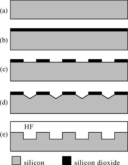
The starting material was an n-doped silicon wafer, h100i oriented, 2.4–4 O cm resistivity, 550 mm thick. A silicon dioxide layer (5000 A˚ thick) was thermally grown on the sample (Fig. 1a and b). A standard photolithographic process was used to defifine the pattern of the initial seeds for electrochemical etching. A BHF etch was then used to transfer the pattern to the silicon dioxide (Fig. 1c). Initial seeds were formed by KOH anisotropic etching through the patterned silicon dioxide (Fig. 1d). When not explicitly stated otherwise, the etch time was long enough to obtain full pyramidal notches. On the same sample, several different patterns (straight lines, square dots and holes, spirals, meander-shaped lines, and others), with different dimensions and pitches were defifined. Electrochemical etching in HF was then used to fabricate regular structures in the patterned substrate (Fig. 1e). The samples were rinsed in deionized water and then dried in a convection oven at 95 8C for 10 min. The samples were fifinally cleaved to allow scanning electron microscope (SEM) observation of the cross-sections.

Fig 1
The experimental setup used for electrochemical etch is described in detail elsewhere [9], and only brieflfly reported here. The front side of the sample is exposed to the electrolyte in a polytetraflfluoroethylene (PTFE) electrochemical cell with a platinum cathode, which is about 5 mm from the sample surface. The electrolyte (HF 48%: C2H5OH 99.9%: H2O, 1:2:17 by volume) is stirred to reduce hydrogen bubble formation. The area of the sample exposed to the electrolyte is about 0.6 cm2 and has a circular shape. Electron–hole pairs are generated by illuminating the back side of the sample with a 300 W halogen lamp, 20 cm from the sample, through a circular window in the metal sheet used to provide the back electrical contact to the sample. The power supply of the lamp can be varied to modulate the etching photocurrent. An HP4145B parameter analyzer was used to apply the anodization voltage and monitor the etching current. All the experiments were executed at room temperature using working current densities J < 30 mA/cm2 and constant anodization voltage of 2.5 V, as suggested in [4] with respect to the measured electropolishing conditions (Jps ¼ 30 mA/cm2 , Vps ¼ 2 V).
上一篇: 单晶锗刻蚀速率的研究
下一篇: 3D-TSV集成的材料和工艺研究进展