Introduction
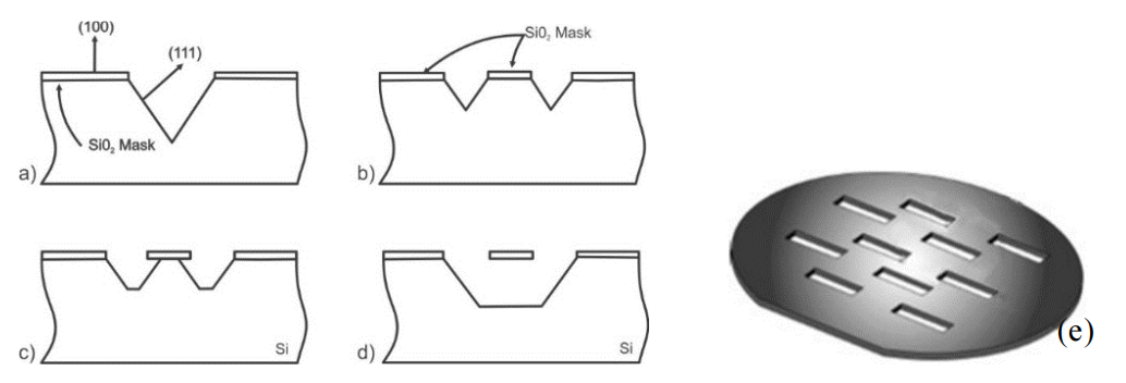
Anisotropic etching of silicon refers to the directional-dependent etching, usually by alkaline etchants like aqueous KOH, TMAH and other hydroxides like NaOH. With the strong dependence of the etch rate on crystal orientation and on etchant concentration and temperature, a large variety of silicon structures can be fabricated in a highly controllable and reproducible manner. Hence, anisotropic etching of <100> silicon has been a key process in common MEMS based technologies for realizing 3-D structures [1-4]. These structures include V-grooves for transistors, small holes for ink jets and diaphragms for MEMS pressure sensors as shown in Figure 1 [1]. The actual reaction mechanism has not been well understood and comprehensive physical and chemical models for the process have not yet been developed. With increasing numbers of MEMS applications, interest has grown in recent years for process modelling, simulation and software tools useful for the prediction of etched surface profiles [4-6].
In this study, test wafers were processed in dilute TMAH in order to etch deep cavities similar to the ones shown below in Figure 1. Due to the large surface areas being etched from the wafers‘ surface, etch byproducts presented a challenge to the process control that produced undesired results. In-line sensors were installed to monitor and control the chemical’s concentration and mass of etch byproducts in real-time. Algorithms were developed to offset the effect of these factors and produced consistent results. The purpose was also to lower the overall cost of ownership (COO) of the process.

Figure 1
Experimental
Wet chemical processes were conducted on a fully-automated GAMA™ wet processing station using 200mm wafers with a typical cavity structure. TMAH was used as the alkaline etchant at a concentration suitable for achieving a maximum etch rate. Silicon etching processes were conducted with the aid of Akrion Systems’ in-situ chemical concentration control system. Occasionally, samples of the baths were taken and titrated for comparison to the NIR results. The goal was to fully etch through the wafers by maintaining a consistent etch rate throughout the entire process.
Results and Discussion
Silicon Etch Rates, Theory vs. Experiment.
The chemical reaction for the anisotropic alkaline etching of silicon is well known and a variety of etchants can be used for the process (KOH, NaOH, TMAH). However, CMOS fabs typically cannot use metal hydroxides as the metal ions will (e) Solid State Phenomena. As a result, TMAH is often used when the metal hydroxides are not allowed.
上一篇: 湿法清洗后氢封端表面的原子级分析