INTRODUCTION
Circuit patterns are transferred to silicon by exposing surfaces of this material to the species formed in fluorine and chlorine-containing plasmas. The physics and chemistry associated with these processes have been studied for many years, and in broad form they are understood. The elementary interactions of free halogen and halogen-containing species with silicon are discussed below, and in turn they are connected to the complex phenomena and chemical feeds which have been developed for use in semiconductor production lines.
Phenomenological mechanisms of etching
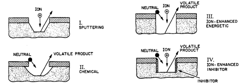
In general, we may divide etching mechanisms into the four basic phenomenological categories shown in Figure 1, sputtering, chemical etching, ion-enhanced energetic mechanisms and ion-enhanced inhibitor processes (refs. 1,2).
Briefly, sputter mechanisms include those in which material is mechanically ejected from a surface by the energy and momentum transferred in energetic ion bombardment. Virtually any material can be sputtered if the ion energy is high and the pressure is low enough for ejected matter to be thrown across the reactor with few collisions. Consequently, pressures on the order of a millitorr or below are required for efficient sputter etching, since the apparatus dimensions are typically some centimeters, and the mean free path of low energy neutral species is about 5/pcm, (p is the pressure in millitorr). Sputtering is unselective and generally slow.

Fig1
The remaining three mechanisms, described in the following, are fundamentally different from sputter removal in at least two ways: a) chemical reactions are central to the the etching process and b) the substrate is converted into volatile, gaseous products. Hence, unlike sputter etching, the other mechanism do not depend on a long mean free path, nor is the amount of material removed sharply limited by the ion current to the surface. A third characteristic of sputtering is the geometrical facets which are produced. While a discussion is beyond the scope of this article, briefly, sputter removal is at a maximum when the surface is inclined about 40" to 60" to ion trajectories; thus sputter-etched planes tend to form along this angle to the surface.
Conditions and mechanism
In many plasma chemistries, the mechanisms described in the first section all can and do take place to some degree. Which process is dominant is heavily influenced by plasma operating parameters such as pressure, excitation frequency, power etc. A comprehensive discussion of these effects is beyond the scope of this article and has been covered elsewhere (refs. 1,2). I shall only highlight a few pertinent trends as they pertain to parallel plate (planar) discharges without a magnetic field. However the effects are very general; while geometry, external fields etc. are important influences, the qualitative phenomena stiU apply.
Silicon etching in fluorine- and chlorine-containing plasmas 1711
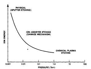
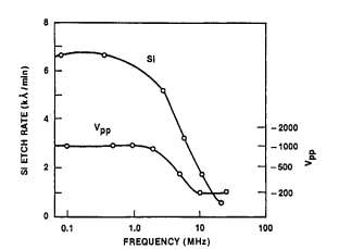
As pressure is decreased below about lOOmTorr, the potential across the discharge characteristically increases, and with this there is a corresponding rise in sheath potentials. At very low pressure, the ion energy is high, reactant density is low and the mean free is long so that sputtering tends to dominate (Fig. 2). At somewhat higher pressure, the ion energy is a bit lower and neutral reactant densities are large enough to support energetic ion-assisted etching. Still higher pressures favor chemical etching and inhibitor ion-assisted directional etching. Excitation frequency has an analogous effect, as shown in Figure 3. Ion energy tends to be moderate when the frequency is above about 3-5MHz, but the potential rises steeply below about 1-3MHz. The etching rate of a substance by energetic ion-enhanced mechanisms will track these variations, as exemplified by undoped polysilicon in a C12 plasma, shown in this figure.

Fig2

Fig3
Etchant must first be formed in the plasma (4) and then adsorbed on the substrate (5). Next, the etchant combines with the substrate to form a volatile product (6, 7), in one of two ways. If spontaneous chemical reaction is fast, as in the case of high& n-doped Si reacting with atomic chlorine, process (6) may dominate. However when the chemical reactions are slow, as in the reaction of undoped Si with C1, ion bombardment may be required to drive the reaction reaction (7, energetic ion-assisted mechanism). Finally, the product formed in these reactions must be desorbed (8). In principle any one of these processes may be a step which controls the overall etching rate. In fact, process conditions may be chosen to intentionally select the rate-limiting step. For example, at low pressure and elevated temperature, doped polysilicon etching will ordinarily be limited by the concentration of etchant (4). But if the process is carried out at low temperature where the silicon chloride reaction product is less volatile, desorption (8) becomes rate-limiting, and reaction product on the sidewall can induce anisotropy (e.g. the inhibitor mechanism with reaction product as the sidewall inhibitor).
上一篇: 微电子应用中的旋涂技术
下一篇: 单晶片兆波系统中的二氧化碳溶解水清洗方法