Experimental
The InGaAsP/InP DH wafers employed were grownby low temperature liquid phase epitaxy (13).Theepitaxial layers were grown on a (001) n-InP sub-strate (~2 X 101 cm-s). The dopant concentrationof each layer was as follows: n-InP (~2 X 1018 cm-3),p-InP (~5 X 1017 cm-3),n-InGaAsP (~5 X 1017cm-3), and p-InGaAsP (~5 X 1017 cm-3).After be-ing degreased and rinsed in deionized water, the n-InPsubstrate was chemically polished with a Brz:CHOHsolution. The thickness of these wafers was about 100um to permit cleavage for the observation of etchingprofiles.
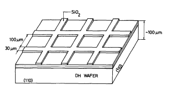
The chemical solutions, eg, Brg:CHOH, usuallyerode photoresists such as AZ-1350.Etchingstudieswere, thus, performed for the etching-selected regionsof the (001) surface InGaAsP/InP DH wafer throughwindows in an SiOz mask (2000A thick) (see Fig.1)The desired geometries, in this case the SiOz stripewidth of 30 um wide, were defined by standard photo-lithography technique using AZ-1350 photoresist andan SiOz etchant of the HF:NHF:HO system.
Acknowledgments
The authors wish to thank T. Suzuki,H Ariyoshi,T. Ikegami,G. Iwane, and H. Nagai for their en-couragement and kind advice throughout this work.
Experimental
The 3 in. diam CZ silicon crystal used in this studywas grown in the <111> direction with boron doping.To ensure thorough examination of bare crystal, heat-treatment for oxygen stabilization was not carried out.The silicon ingot shape is schematically shown in Fig.1. The crystal was dislocation-free, and 24 waferspecimens 2 mm thick were taken from the top portion(Tw), middle portion (MW), and bottom portion(BW).These wafers were individually numbered (1to 24) in sequence for each portion to clarify theoriginal specimen position in the ingot. Longitudinalplate specimens 2 mm thick in the (110 plane parallelto the <111> growth direction were also taken fromthe upper portion (UP) and lower portion (LP) asshown in Fig.1.Both sides of all specimens weremechanically-chemically polished in the usual fashionto remove surface damage.

Fig1
Results
The oxygen concentration in as-grown crystals([Oil) is plotted against the fraction of melt pulled(g) in Fig.1. The oxygen concentration [Oi] changeafter individual annealing at temperatures from 600to 1150°C for 16 or 64 hr in a dry Oz atmosphere isshown in Fig. 2. Specimen wafers were selected fromthe top (TW),middle (MW),and bottom (BW) por-tions as shown in Fig. 1. For 16 hr annealing,adistinctive [Oi] change was observable in the TWspecimen; however,no [Oi] change is observed inspecimens with low[Oi]。 (less than 14 X 1017 atoms/cm3) For 64 hr annealing, in addition to the even moremarked change in the TW specimen than in 16 hr an-nealing a slight decrease in [Oi] is found at 1000C foreven lowlOila specimens.
Plate specimens shown as UP in Fig.1 were annealedat 750° or 1000C for 64 hr in a dry O, atmosphere, The[Oi] change in the plate annealed at 1000°C is shownin Fig. 3. It is quite evident that the higher oxygenconcentration [Oi]。 results in the greater oxygen pre-cipitation when heat-treatment conditions are constant.
上一篇: EUV掩模的碳污染对光刻性能的影响
下一篇: 碳化硅器件加工过程化学浓度控制