1. Introduction
5G is the next generation of mobile networks and will achieve speeds of several Gb/s. 5G is therefore designed to support large amounts of data, but also to enable a very large number of connections and multiply the types of uses. It will be versatile, to adapt to the needs of each use: performance, energy savings, critical uses (e.g. autonomous cars), etc. For 5G, centimeter and millimeter waves are considered because they have wide ranges of available spectra (3.5–6 and 24–86 GHz) and will also bring new features such as beam forming and Multiple Input Multiple Output (MIMO) antenna arrays.
The choice of 5G technology blocks is critical to ensure the required performance. Despite the excellent performance of emerging materials, silicon-based technologies remain a strategic choice for RF applications. The co-integration of high-speed digital circuits alongside analog and RF front-end modules on the same chip, the excellent control of the silicon process and the low production cost of the substrates are some advantages of silicon technologies. A substrate technology enabling such integration and providing a platform for RF and mm-wave circuitry is desired to be low-loss, highly isolating, and highly-linear.
As an alternative to TR-SOI, porous silicon (PSi) has been proposed for several decades. This material is formed by electrochemical dissolution (anodization) of bulk silicon. PSi achieves high resistivity, low permittivity, low losses, low crosstalk levels, and strong linearity. For all these reasons, PSi is a promising candidate for RF substrates. Substantial amounts of work have proved PSi to be a promising candidate as RF substrates [3–21], however, the incompatibility of porous silicon with high temperature annealing (cracking or bending in the substrate) makes its integration in to a full CMOS process impossible with suffiffifficient yield.
2. Substrate description
To benchmark the newly developed POST-PSi substrate and evaluate its performance, it is compared to the two most widely used RF substrate technologies in the RF industry today: the HR-SOI and TR-SOI substrates. In this section the physical structures and fabrication processes of each substrate are described.
2.1. High resistivity substrate (HR)
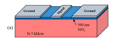
The HR substrate is based on an n-type silicon wafer with a nominal resistivity above 5 kΩ cm. A 500-nm silicon dioxide (SiO2) layer is deposited at 300 °C by plasma-enhanced chemical vapor deposition (PECVD), followed by a 1-μm-thick layer of aluminum deposited by physical vapor deposition (PVD) for the defifinition of the CPW line devices by standard photolithography and wet etching. A typical HR substrate structure is depicted in Fig. 1(a).
2.2. Trap-rich substrate (TR)
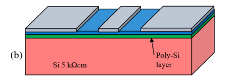
The TR substrate consists in an n-type HR-Si wafer with a nominal resistivity above 5 kΩ cm and a 300-nm-thick poly-Si layer rich in traps and defects deposited through low-pressure chemical vapor deposition (LPCVD). On top, a 500-nm SiO2 layer is deposited at 300 °C by PECVD, followed by a 1-μm-thick layer of aluminum deposited by PVD for the defifinition of the CPW lines. A typical TR substrate structure is depicted in Fig. 1(b).


Fig1
2.2. Trap-rich substrate (TR)
The TR substrate consists in an n-type HR-Si wafer with a nominal resistivity above 5 kΩ cm and a 300-nm-thick poly-Si layer rich in traps and defects deposited through low-pressure chemical vapor deposition (LPCVD). On top, a 500-nm SiO2 layer is deposited at 300 °C by PECVD, followed by a 1-μm-thick layer of aluminum deposited by PVD for the defifinition of the CPW lines. A typical TR substrate structure is depicted in Fig. 1(b).
3. RF characterization at room temperature On-wafer measurements of CPW lines were performed using an Agilent 2-port performance network analyzer (PNA)-X vector network analyzer and a pair of ground-signal-ground (GSG) Infifinity probes from Cascade Microtech with 150 µm pitch. Short-Open-Thru-Load (SOLT) calibration method is used to calibrate the system at the probe tips for better accuracy of the measurement. The lines are 8 mm-long, the signal and ground widths are 38 and 208 μm-wide, respectively, and the spacing between the signal and ground lines are 18 μm-wide. The CPW electrical parameters are extracted using the methods described in [22,23].
上一篇: 晶圆级芯片封装可靠性的提高
下一篇: 硅的等离子体化学刻蚀