I. INTRODUCTION
The progress in development nano- and microelectromechanical devices and systems promises the same revolution in engineering, what was made by microelectronics in electronics [1]. A basis of microelectromechanics is the association of superficial microprocessing advanced in microelectronic technology, with volumetric processing and use of new materials and physical effects. The new volumetric constructive elements - membrane, beam, cavity, aperture with the large thickness are created. It has supplied progress in the field of microengines, microrobots, micropumps, supersensitive of the sensors of various physical parameters (of pressure, acceleration, temperature and others), microoptics.
II. TECHNOLOGICAL ASPECTS OF DEVELOPMENT NANO- AND MICROELECTROMECHANICAL SYSTEMS
The opinion is standard, that practical use of the high vacuum of plasma etching in technology of microelectronics considerably outstrips study of physicschemical processes proceeding at processing of materials chemically by active plasma [2]. The existing theoretical descriptions of mechanisms of vacuum-plasma etching are while obviously not sufficient.
III. THE CONTROL OF THE COORDINATION VF OF THE GENERATOR WITH SYSTEM PCE SI
On equipment “Plasma 600” the control of the coordination of internal resistance VF of the generator with complete resistance (impedance) of system of etching is carried out on a current of a grid. It is considered, that maximal a current of a grid corresponds to a resonance of a contour of inductance. Only in this case VF the generator will have good efficiency and to give back in loading rated power [6].
The analysis of dependences shows, that the adjustment of process of etching of silicon on a maximum of a current of the gauge allows to receive higher velocity of etching thus an anode current. It is possible to explain it to that at such way of adjustment on a resonance in plasma is entered more capacity, i.e. the efficiency is higher.
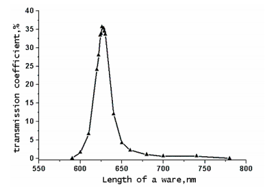
Thus there is a coordination of processes of radiation of the molecules, exited by the category, of working gas and of plasma chemical of etching of silicon. Therefore adjustment of a resonant contour of installation was carried out so that at the given anode current the current of the gauge was maximal. And as the gauge represents the photo diode, the current will be maximal at the maximal flow of radiation of the molecules, exited by electronic impacts, of working gas. In the present researches on the photo diode the radiation through interference the light filter with λmax = 626 nm acted.
IV. RESEARCH OF LOADING EFFECT
The speed of etching, as a rule, is proportional to concentration CAP, therefore it will decrease the stronger, than more wafeы is in plasma. For research of loading effect the samples which have been cut out from a silicon plate were used КДБ 4,5 (100). The sizes of samples were equal: 5x5 mm2 , 5x10 mm2 and 5x15 mm2 . The increase of the area was reachedor by joint etching of several samples. Samples settled down approximately on 4 - 5 сm from the left edge of the reactor on the centre. The etching was made in quartz reactor with covered fluorine polimer by walls.
The research of loading effect was carried out in two modes of stabilization of process: one was supported and too meaning of an anode current and one was supported and too meaning of a current of the sensor at change of the area of samples.
Thus in a range of the areas from 25 mm2 up to 100 mm2 the loading effect is absent. At the greater area of samples the speed of etching decreases from 6 µ m/min up to 3,73 µ m/min. The control of process of etching on a constant current of the anode or on a constant current of the sensor has given approximately identical result, that speaks about good stability of process of plasma etching of silicon in the chosen range of parameters.

Fig1
The given mode poorly has shown itself in a case of the photoresist mask, as the organic materials completely burn out in the plasma, enriched with oxygen, is especial in case of long process, in view of strong devil of a plate both more intensive oxidation and burning out of the organic. Therefore further the aluminium mask by thickness of the order of the micron, put by a method of the thermal evaporate was used.
The dependence of speed of etching on an anody current was investigated under following conditions: the sample of silicon КЭФ 7.5 (100) area 11,75 cm2 is at the centre of the reactor. A flow of oxygen 30 units, flow CCl2F2 50 units, pressure in the reactor 15 units. Time of etching 5 minutes.
上一篇: 用于5G应用的后处理多孔硅
下一篇: 化学清洗过程中重金属污染的监测方法