The continuing increase of integrated circuit (IC) complexity, and the reduction of critical dimension that requires reduction of gate oxide thickness, generates a need for better control of heavy metal contamination. Published data on acceptable contamination levels, that do not deteriorate gate oxide integrity, are 1012 cm 2 for 1.25 Fm technology (200 A oxide thickness) 1 and 10 l~ cm 2 for 0.5 ~msses, incom technology (125 A oxide thickness). 2 By the end of this decade the acceptable limits will probably be reduced to 108 cm-2.3 This puts stringent demands on cleaning methods and characterization techniques. There is an urgent need for a fast, inexpensive, high-throughput measurement method that can be used as a quality control (QC) method to qualify, in real-time, cleaning proceing chemicals, chemicals at point of use, and performance of cleaning stations.
Here we explore the application of surface photovoltage (SPV) to monitor chemical cleaning. Compared to other technologies such as total reflectance x-ray fluorescence spectroscopy (TXRF) or atomic absorption spectroscopy (AAS), the application of SPV for monitoring cleaning processes is rather new, although some impressive strides have already been made. The major advantages of the SPV approach over traditional techniques are: capability of contactless measurements on patterned (product) wafers, no sample preparation is required, and short measurement times (on the order of seconds) which allow real-time feedback, and unmatched sensitivity (on the order of 109 cm -2 for Fe).
Principles of surface photovoItage.--In the constant photon flux SPV method, minority carrier diffusion length is determined from a spectral dependence of the surface photovoltage, h V, and specifically from a dependence of i V on the light penetration depth, ~-1, where ~ is the absorption coefficient. 4 A depletion (or inversion-depletion)-type surface barrier (shown in Fig. i for an n-type semiconductor) is best suited for measurement. This assures preferable collection of the excess minority carriers in the surface space-charge region, while the majority carriers are repelled from the surface and play an insignificant role. In this method the accumulation of minority carrier should be a predominant mechanism leading to the surface photovoltage.
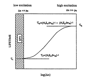
To avoid unambiguity related to the dependance of lifetime on the generation rate, SPV measurements were carried out under conditions of very low excitation, 101~ to 1013 photon/cm 2 per second. For these generation rates an excess minority carrier concentration in n-type 10 ft-cm silicon with lifetime of 10 -~ s (100 ~m diffusion length) is on the order of 108 to 101~ cm -3, which is 10 7 to 10 5 of majority carrier concentration. It has to be pointed ,out that this generation rate is 106 to 10 ~ times lower than the generation rates used in lifetime measurement methods using laser generation (e.g., PCD microwave reflectance or ELYMAT). Dependence of lifetime on generation rate, shown in Fig. 2, demonstrates that a significant difference in the measured values of the lifetime at low and high generation rates could exist. The change of lifetime with generation rate is a function of majority carrier concentration and characteristic of recombination centers present in silicon. As was pointed out by Zoth, 8 in the case of Fe measurements, results obtained at low generation rates are not transferable to high generation rates. The procedure for Fe measurements and Fe calibration curves developed for low generation rates and discussed below are not transferable to other lifetime measurement techniques which use high generation rates.

Fig1
In order to monitor the efficiency of cleaning processes by bulk contamination measurements, one has to drive into the bulk heavy metals left on the surface of a silicon wafer with a high-temperature annealing. The time and temperature of this high-temperature annealing should be such that heavy metals left on the silicon surface will dissolve in silicon (their concentration will be lower than the solubility limit) and time will be sufficient to distribute them uniformly through the silicon wafer. Figure 8 shows time, at a given temperature, for various heavy metals required to diffuse through wafer thickness and calculated using published diffusion constants? During these calculations we assumed that heavy metals are driven from the front and back surface of a silicon wafer.
上一篇: 硅的等离子体化学刻蚀