1. Introduction
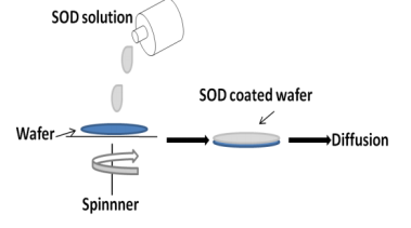
During last decades, the researcher mainly focused on cell efficiency improvement and watt peak cost reduction for crystalline silicon solar cells. Most of PV industries use the standard fabrication process for the reduction of the process cost. The emitter is the most important part and the formation of emitter constitutes a crucial step in the manufacturing of the crystalline silicon solar cells. In case of crystalline silicon solar cell processing, carrier diffusion into p-type or n-type wafer creates emitter formation. For emitter formation the most used technique in photovoltaic industry is POCl3 diffusion in cylindrical quartz tube. Spin-on dopants (SOD) also provide an impurity source for semiconductor junction as well as emitter layer fabrication.
In this work, our goal is to put an intermediate step in between lab-scale fabrication and fully automated commercial facilities or processes. That’s why, the principal motivation is to put stress on the simplicity and the cost effective fabrication process. The use of low cost commercial CZ wafers and the use of SOD instead of doping gas POCl3 can made this work interesting for a low budgeted and industrially compatible fabrication process of solar cells. Eventually, smaller fabrication facilities may be benefited from these comparative studies and get involved in more human resource involved manufacturing around the world to make this technology reachable to all with reduced production cost.
2. Related Works
Lachiq et al. reported a fabrication scheme where the authors used a spin on dopant solution to obtain diffusion with a rapid thermal annealing process in an inert atmosphere. The authors retained the thin (<20 nm) SOD film to serve as a surface passivation layer with further need for an ARC [4].
Vikram et al. at University of Virginia in 2010 demonstrated a simplified and single step process on P-type CZ–Si and FZ–Si wafer for photovoltaic device fabrication. Single step process incorporates doping, anti-reflection coating (ARC) and a surface passivation layer. P5O9 was served as the dopant solution for photovoltaic device fabrication [5].

Fig1
Edge Isolation The Phosphorus doped layer covers the entire surface including edges. It is important to disconnect the front emitter from the back contact through etching the edges of the sample. Several processes are involved such as chemical etching, plasma etching, laser cutting, mechanical sawing, grinding with sand paper, single side etching etc. In this research single side etching and laser cutting techniques were used. For the single side etching, HF/HNO3 acid barrier paste was used. It was carried out by screen printing process. Samples were heated by 120°C for 10 minutes by oven. Advantages of single side etching are preserving the active cell area, lower parasitic loss, higher FF compared to laser isolation process [3].
The four point probe apparatus is one of the standard apparatus for the measurement of resistivity of semiconductors. If the sample is in the form of a thin wafer or the form of a thin semiconductor material deposited on a substrate then it is also useful for the measurement.
上一篇: 磷酸电解液中铜电解抛光的机理研究